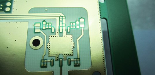
With the requirement of PCB heat dissipation capacity for high intensive electronic components and high-power electronic components, the industry has introduced embedded copper coin PCB technology. Using the high thermal conductivity of copper coin, the heat generated by the parts in the PCB is transferred to copper coin quickly, and then the heat is dispersed in the air through copper coin.
The embedded copper coin is embedded in the PCB slot after routing and metalized when finished PCB lamination. PCB and copper coin tightly connected through both the amount of embedding, and the electrical connection is achieved by copper plating, which makes the overall heat dissipation performance good. The article will analyse and improve the embedded copper coin PCB technology from the aspects of copper block design, size compensation and press control to ensure the quality and efficiency of PCB product.
Embedded copper coin PCB widely used and meets the heat dissipation requirements of more and more intensive components and high-power components with high thermal conductivity of copper coin.
According to the way of copper coin and PCB connection, it can be divided into buried copper coin PCB and embedded copper coin PCB.
The embedded copper coin PCB means insert the copper coin into the PCB slot after finished routing and metalized after PCB press. PCB is tightly connected with copper coin through the embedding quantity between them, and the electrical connection is achieved by copper plating.
The buried copper coin PCB means buried copper coin into pre-milling groove when pressing. The copper coin and PCB are connected by laminated prepreg.
The embedded copper coin directly contacts with the inner copper layer and air, heat transfers to the copper coin quickly when PCB using. Then the heat is removed from the air through the copper coin. The heat dissipation effect is better than buried copper coin PCB, the process is less, the cost is lower, and the application prospect is broad. However, the PCB technology of embedded copper coin is not mature, and the technology is difficult. It is prone to produce reliability problems, which greatly affects the extensive application of PCB copper coin.
Description of process difficulties
The technology of embedding copper coin is to insert copper coin into the metallized wall of PCB after PCB press. The processing flow is as follows:
Material sheet cutting—-Inner layer making—Brown treatment—Laminated pressing—X-RAY drilling target—Milling groove—Groove metalizing—embedding copper coin—Grinding—Drilling—P.T.H.—First plating—Outer layer making—Solder mask printing—Silkscreen printing— Re-solidifying—ENIG— Test—FQC—Shipping
The embedding of copper coin is a key process, need matching the copper coin shape design, copper coin and PCB milling groove dimension.Smoothness and other technical difficulties, otherwise it is easy to produce reliability problems.
1.Copper coin design: copper coin shape design affects the embedding effect of copper coin, resulting in damage to copper coin and groove wall, also high scrap.
2.The groove size of the base plate is not consistent with the compensation design of the copper coin size, and can’t achieve the common wear of the copper coin and the groove wall, lead to embedded copper coin and substrate wall can not be closely contacted, the copper coin pushing force is low or serious wear.
3. The problem of smoothness of embedded copper coin: the flatness of copper coin can not meet the general requirements of component surface (CS surface) (-50 to +100) um and welding surface (SS surface) (-150 to +150) um, leading to excessive height difference will greatly reduce the heat dissipation effect of electronic components and copper coin.
Process improvement solution
1. The most suitable size of copper coin and PCB is 0-0.2 mm. Copper coin and groove wall wear and insert force are moderate, copper coin embedded smoothly. Otherwise, too small will cause copper coin not contact closely with the groove wall.
2. Excessive size will cause damage to the wall and copper coin, and risk of copper being unable to be embedded.The groove size accuracy is controlled at + 0.075 mm, and the copper coin size is compensated by 0.075 mm for milling groove size.
3. Copper coin design: Copper teeth, fillet and round edge design, copper tooth height, fillet and round edge size O.2 mm, machining tolerance of + 0.05 mm
4. PCB milling compensation: groove size must be smaller than copper coin size 0.075mm (unilateral compensation -0.038mm), slot size error + 0.075mm.
Control of copper block Flatness:
(1.)According to our specification, we should design the thickness and structure of product lamination normally.
(2.)According to the theoretical thickness calculation, 2 bits after the decimal point are calculated, and the second bits after the decimal point are calculated by “less than 5 according to 5, greater than or equal to 5 into 1 bits”.
(3.) It is necessary to use a suitable fixing method, platoon pattern and compression parameters for copper block embedding;
(4.) The copper block should be embedded from the surface of the element (higher level of evenness) and meet the planeness requirements of the surface of the element and the welding surface.
Review of the main technical difficulties in the processing of PCB products embedded in copper coin, we find out the reasons and optimize them. Combination of test results and production verification,it has effectively improved the defects such as groove wall damage, poor adhesion and poor smoothness in the processing of PCB products embedded in copper coin.
Submit a quote for your specific PCB requirements or Contact us if you would like to arrange a tour of our production facility. Our email address: [email protected] . Skype ID: [email protected] . WhatsApp: +8613392412348. And our sales and engineer team will response to you once receive your quotation!