A PCB surface finish is crucial for a printed circuit board as it prevents the copper (exposed traces, pads, holes and ground plains) from oxidation – a critical ingredient to high-level application performance.
A surface finish is essential for making a reliable connection between the PCB and the electronic component. A surface finish has two major functions, to provide a solderable surface for sufficient soldering components to the PCB, and to protect any exposed copper from oxidizing.
When it comes to choosing the right type of final surface finish, it is just as important as selecting the right material for your bare board. Selecting the correct surface finish for your application is critical for performance. For assistance with selecting a surface finish, send our trusted engineers an email or call.
With increasing demands for thin, high-density, fast speeds, and lightweight applications, the solder finish will make all the difference.
Modern surface finishes are lead-free, in accordance with Restriction of Hazardous Substances (RoHS) and Waste Electrical and Electronic Equipment (WEEE) directives, and include:
- ENIG (Electroless Nickel Immersion Gold)
- ENEPIG (Electroless Nickel Electroless Palladium Immersion Gold)
- Electrolytic Nickel/Gold – Ni/Au (Hard/Soft Gold)
- Immersion Silver
- White Tin or Immersion Tin
- Lead Free HASL (Hot Air Solder Leveling)
- OSP (Organic Solderability Preservatives)
Choosing the correct PCB surface finish for your application requires taking factors into account like cost, the final application environment (e.g. high-heat/thermal, vibration/stability, RF), component density/selection, lead/lead free requirements, shelf life, shock/drop resistance, production volume, and throughput.
Due to the increased demand for improved performance of electronic applications, surface finishes have also been upgrading. Because of tighter PCB topography the HASL surface finish is quickly being replaced by gold-based surface finishes like ENIG, ENEPIG, and soft/hard gold. The gold-based surface finishes have a lot to offer in terms of features and benefits when used in applications.
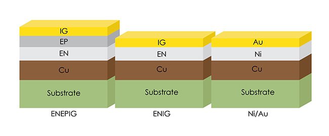
Diagram illustrating the difference between ENIG and other surface finishes
ENIG (Electroless Nickel Immersion Gold)
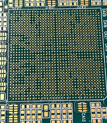
Example of an ENIG Surface Finish on PCB
ENIG consists of two layers of metallic coating, which are deposited on the copper surface through chemical process, 2-5μ inches of immersion Gold (Au) over 120-240μ inches of electroless Nickel (Ni).
The nickel layer protects the copper from oxidation, and the gold layer protects the nickel layer. This dramatically increases the resistance to corrosion and also maintains a flat surface which is crucial for assembly of leadless components. ENIG usage has become very common now due to the accountability for lead-free regulations.
ENIG (Electroless Nickel Immersion Gold)
| PROS | CONS | MOST COMMON USES |
| Flat Surface – Excellent for Assembly of Dense Topography PCBsLong Shelf LifeGreat for Plated Holes and Fine Pitch / BGA / Small ComponentsWire Bondable (When Aluminum Wire Is Used)High Temperature Resistance | ExpensiveSignificant Signal LossUnable to ReworkBlack Pad / Black NickelNot Suitable for Touch Contact Pads | High Density PCBsRigid PCBsFlex PCBsIndustries: Consumer, Data/Telecom, Aerospace, Military, High Performance, and Medical |
Properties of ENIG
| Properties | ENIG |
|---|---|
| Contact Applications | Yes |
| Deposit | Immersion |
| Exposed Copper | No |
| Handling | Normal |
| Process Control | Fair |
| Process Cost | Medium |
| Required Thermal Cycles | >2 |
| Shelf Life | Long (1+ Years) |
| SMT | Flat |
| Thickness | 3 – 10 µin of Gold over 150 – 200 µin of Nickel |
| Thin Board Finish | Yes |
Applications of ENIG
| Applications | ENIG |
|---|---|
| BGA & μBGA | Yes |
| Contact/Connector | Yes |
| Fine Pitch SMT | Yes |
| Flip Chip | Yes |
| High Reliability | High |
| RoHS Compliant | Yes |
| Solder Joint Integrity | Good |
| Wire Bonding | Yes (Al) |
ENEPIG (Electroless Nickel Electroless Palladium Immersion Gold)
ENEPIG is probably not new to you, but it is a surface finish that has become increasingly popular recently due to the price reductions in palladium. It also has increased in popularity and use because of its many features and benefits. It also has a distinct advantage over the ENIG surface finish, which we’ll get into below.
The ENEPIG surface finish is composed of four metal layers:
- Copper
- Nickel
- Palladium
- Gold

Diagram illustrating the difference between ENEPIG and other surface finishes.
The difference between ENEPIG and ENIG is the added layer of palladium. The palladium helps protect the nickel layer from corrosion, which helps prevent “black pad” from occurring. This is one of the distinct advantages of ENEPIG over the ENIG surface finish. The immersion gold layer that sits atop the palladium offers nearly-complete board protection by protecting and preserving the palladium underneath.
When compared to other surface finishes, like hard gold and soft gold plating, ENEPIG has become more affordable in recent years. The cost of the ENEPIG surface finish decreased because the added palladium layer reduces the required thickness of the more expensive gold layer.
ENEPIG is Capable of Your Demanding Requirements
The ENEPIG finish is capable of the majority of the ultra-demanding requirements with multiple package types like, through-holes, SMT, BGA, wire bonding, and even press fit.
The ENEPIG surface finish is capable of ultra-demanding requirements.
The PCB surface finish with ENEPIG is very thin (between 0.05μm and 0.1μm), making the assembly and soldering process very simple and definitely more reliable when compared to ENIG. ENEPIG also has a long shelf life due to its durability and resistance from tarnishing.
| ENEPIG (Electroless Nickel Electroless Palladium Immersion Gold) | ||
| PROS | CONS | MOST COMMON USES |
| Black Pad FreeGood for Touch Contact / Push ContactHigher Reliability Wire Bonding than ENIGStronger Solder Reliability than ENIGCheaper than Electrolytic GoldLead Free & RoHS CompliantLong Shelf LifeMultiple Reflow Soldering CapabilityFlat Surface – Excellent for SolderabilityGreat for Plated Holes and Fine Pitch / BGA / Small ComponentsEasier Inspections | More Expensive than ENIGMay Not Be As Reliable for Gold Wire Bonding When Compared to Soft Gold | Multi-Layer PCBsHigh Density AssembliesMixed Package TechnologiesIndustries: Military, Medical, Aerospace, High Performance Devices |
Properties of ENIG
| Properties | ENEPIG |
|---|---|
| Contact Applications | Yes |
| Deposit | Immersion |
| Exposed Copper | No |
| Handling | Normal |
| Process Control | Fair |
| Process Cost | High |
| Required Thermal Cycles | >2 |
| Shelf Life | Long (1+ Years) |
| SMT | Flat |
| Thickness | 1 – 2 µin of Gold over 4 – 8 µin or 8 – 15 µin Palladium over 100 -150 µin Nickel |
| Thin Board Finish | Yes |
Applications of ENEPIG
| Applications | ENEPIG |
|---|---|
| BGA & μBGA | Yes |
| Contact/Connector | Yes |
| Fine Pitch SMT | Yes |
| Flip Chip | Yes |
| High Reliability | High |
| RoHS Compliant | Yes |
| Solder Joint Integrity | Good |
| Wire Bonding | Yes |
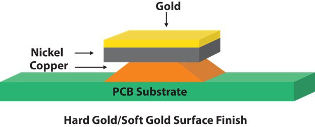
Electrolytic Nickel/Gold – Ni/Au (Hard/Soft Gold)
Depending on applications, printed circuit board technologies use gold extensively. Gold has good electrical conductivity, tarnish resistance, solderability after storage, and being excellent etch resist.
Electrolytic Ni/Au has a layer of gold plating over a base of electroplated nickel. The purity of the gold plating categorizes this finish as either hard gold (99.6% purity) or soft gold (99.9% purity). The choice of hard gold versus soft gold depends on the type of application you are looking to create
Examples of the Hard/Soft Gold Surface Finish
Hard Gold Surface Finish
Hard gold is a gold alloy with complexes of cobalt, nickel or iron. A low-stress nickel is used between gold over-plating and copper. Hard gold is not suitable for wire bonding.
We recommend using the hard gold surface finish for components and applications with heavy usage and a high likelihood of wear and tear, like:
- Interconnected Carrier Boards
- Edge Connector Fingers
- Keypads
- Contacts
The thickness of the hard gold surface finish will vary depending on the applications. When hard gold is used for compliance in military applications, the minimum thickness shall be 50 -100 micro inch.
Nonmilitary applications require 25 to 50 micro inches. Here are the recommended minimum and maximum thickness values:
- 17.8 μin is recommended for IPC maximum solderable thickness
- 25 μin gold over 100 μin nickel for IPC Class 1 & Class 2 applications
- 50 μin gold over 100 μin nickel for IPC Class 3 applications
Properties of Hard Gold
| Properties | Hard Gold |
|---|---|
| Contact Applications | Yes |
| Deposit | Electrolytic |
| Exposed Copper | Yes |
| Handling | Normal |
| Process Control | Fair |
| Process Cost | High |
| Required Thermal Cycles | >2 |
| Shelf Life | Long (1+ Years) |
| SMT | Flat |
| Thickness | 98% Pure, 23 Karat 30 – 50 µin over 100 – 150 µin of Nickel |
| Thin Board Finish | Yes |
Applications of Hard Gold
| Applications | Hard Gold |
|---|---|
| BGA & μBGA | Yes |
| Contact/Connector | Yes |
| Fine Pitch SMT | Yes |
| Flip Chip | Yes |
| High Reliability | Medium/High |
| RoHS Compliant | Yes |
| Solder Joint Integrity | Poor |
| Wire Bonding | No |
Soft Gold Surface Finish
A soft gold finish, as the name suggests, contains a higher gold purity on the outer gold plating. Soft gold has a 99.9% purity.
An example of the soft gold surface finish on a PCB
Soft gold finish is used for boards designed mostly for applications that require wire bonding, high solderability and weldability. Soft gold produces a much stronger welded joint when compared to hard gold.
Electrolytic Ni/Au has a layer of gold plating of varying thickness
Generally speaking, and with all other factors being equal, Electrolytic Nickel/Gold is the most expensive PCB surface finish. However, some applications do require the Electrolytic Nickel/Gold surface finish.
Properties of Soft Gold
| Properties | Soft Gold |
|---|---|
| Contact Applications | Yes |
| Deposit | Electrolytic |
| Exposed Copper | No |
| Handling | Normal |
| Process Control | Fair |
| Process Cost | High |
| Required Thermal Cycles | >2 |
| Shelf Life | Long (1+ Years) |
| SMT | Flat |
| Thickness | 99.99% Pure, 24 Karat 30 – 50 µin over 100 – 200 µin of Nickel |
| Thin Board Finish | Yes |
Applications of Soft Gold
| Applications | Soft Gold |
|---|---|
| BGA & μBGA | Yes |
| Contact/Connector | No |
| Fine Pitch SMT | Yes |
| Flip Chip | Yes |
| High Reliability | High |
| RoHS Compliant | Yes |
| Solder Joint Integrity | Poor |
| Wire Bonding | Yes (Au) |
Immersion Silver Surface Finish
Immersion Silver (also called immersion Ag) is a RoHS compliant (lead-free) surface finish that is an ideal choice for flat surface requirements and fine pitch components with reasonable costs. This surface finish can also replace Immersion Gold over Electroless Nickel (Au/Ni) for most applications. And the thickness ranges from 0.12 to 0.40 μm.
It has a decent shelf life of 6 to 12 months, but it can be sensitive to contaminants found in the air and on some surfaces. This makes it critical to have a highly qualified boardhouse to properly control and expedite the board packaging process. This surface finish is also subject to tarnishing, which is something to take into account.
As mentioned above, common applications include flat surface requirements, which may include:
- Membrane Switches
- EMI Shielding
- Aluminum Wire Bonding
- Very Fine Traces
Immersion Silver
| PROS | CONS | MOST COMMON USES |
| RoHS CompliantPlanarGreat for Fine Pitch / BGACost EffectiveHighly StableSimple ProcessingVery Flat SurfaceReworkableExcellent Solderability | Subject to TarnishingSilver Metal WhiskeringHigh Friction CoefficientSensitive to ContaminantsStrict Storage and Handling RequirementsWelding Issues with Micro-HolesProne to ElectromigrationDifficulty with Electric Testing |
Properties of Silver
| Characteristics | Silver |
|---|---|
| Contact Applications | No |
| Deposit | Immersion |
| Exposed Copper | No |
| Handling | Critical |
| Process Control | Fair |
| Process Cost | Medium |
| Required Thermal Cycles | >2 |
| Shelf Life | Medium (9-12 Months)* |
| SMT | Flat |
| Thickness | 6 – 18 µin |
| Thin Board Finish | Yes |
*Requires Unique Storage Techniques µin = Microinches
Applications of Silver
| Applications | Silver |
|---|---|
| BGA & μBGA | Yes |
| Contact/Connector | No |
| Fine Pitch SMT | Yes |
| Flip Chip | Yes |
| High Reliability | Medium/High |
| RoHS Compliant | Yes |
| Solder Joint Integrity | Excellent |
| Wire Bonding | No |
Immersion Tin (Also known as White Tin)(ISn)
What is Immersion Tin?
Immersion Tin is a is a RoHS compliant (lead-free) surface finish that is an ideal choice for flat surface requirements and fine pitch components. White Tin (Immersion Tin) is a deposit of a thin layer of Tin on Copper layer of a PCBs. It is not used as often as other surface finishes because not all PCB manufacturers offer it. The flatness of this particular coating makes this an ideal surface finish choice for small geometries and components.
Tin also is the least expensive type of immersion coatings. Although it is an economical choice, it does come with some drawbacks.
It’s Not Without Its Drawbacks
Immersion Tin has its advantages, but there are a few disadvantages to using this surface finish. As you may know, Copper and Tin have a strong affinity for one another. This means, over time, diffusion of one metal into the other will occur. It directly impacts the shelf life of the Immersion Tin deposit and ultimately the performance of the ?nish.
Immersion Tin has a limited shelf life, 3-6 months. For the best results assembly (soldering) shall happen during 30 days.
Tin Whiskering is also another downside to using Immersion Tin as a surface finish. The negative effects of tin whiskers growth are well described in industry related literature and topics of several published papers.
The Immersion Tin finish is not very durable, therefore, PCBs with Immersion Tin finish must be handled with caution.It provides a consistently flat surface approximately 20-40 micro inches in thickness.
Why Is It Used?
Immersion Tin has been primarily used as an alternative to a lead-based surface finish. It is also used for its very flat and smooth finish making it ideal for fine geometries and fine pitch surface mount components.
Another reason to use immersion tin is sustainability. Elements that may be difficult to source on a consistent basis are used in other finishes, such as ENIG or HASL. Additionally, it uses less water and chemicals in the application process.
It is also easier to re-work.
As with all of the surface finishes we’ve compared so far, there are a number of advantages and disadvantages. Here are the advantages and disadvantages for Immersion Tin.
Advantages:
- Immersion Tin Finish allows excellent flatness (suitable for SMT), good for fine pitch / BGA / smaller components
- Immersion Tin has mid-range cost for lead-free finish
- Press fit suitable finish
- Retains good solderability after multiple thermal excursions
- Suitable for horizontal production line.
- Suitable for fine geometry processing, lead-free assembly.
Disadvantages:
- Sensitive to handling.
- Short shelf life, tin whiskering can occur after 6 months
- Aggressive to solder masks
- Not recommended to use with peelable masks
- Not a suitable choice for a contact switches.
- Special setting requires (soft probe landing) for electrical test
Here is a full table with some of the pros and cons along with some of the most common uses for the Immersion Tin surface finish.
Immersion Tin
| PROS | CONS | MOST COMMON USES |
| RoHS CompliantGreat for Fine Pitch / BGACost EffectiveHighly StableSimple ProcessingVery Flat SurfaceReworkableExcellent Solderability | Subject to TarnishingSilver Metal WhiskeringHigh Friction CoefficientSensitive to ContaminantsStrict Storage and Handling RequirementsDifficulty with Electric Testing |
Properties of White Tin
| Properties | White Tin |
|---|---|
| Contact Applications | No |
| Deposit | Immersion |
| Exposed Copper | No |
| Handling | Normal |
| Process Control | Fair |
| Process Cost | Medium |
| Required Thermal Cycles | >2 |
| Shelf Life | Medium (9-12 Months)* |
| SMT | Flat |
| Thickness | 25 – 60 µin |
| Thin Board Finish | Yes |
*Requires Unique Storage Techniques µin = Microinches
Applications of White Tin
| Applications | White Tin |
|---|---|
| BGA & μBGA | Yes |
| Contact/Connector | No |
| Fine Pitch SMT | Yes |
| Flip Chip | Yes |
| High Reliability | Medium |
| RoHS Compliant | Yes |
| Solder Joint Integrity | Good |
| Wire Bonding | No |
HASL & Lead Free HASL (Hot Air Solder Leveling) / Sn/Pb
Hot Air Solder Leveling (HASL) is one of the most commonly used surface finishes in the industry. HASL is divided into two types, and there are two types because one contains tin with lead and the other contains tin without lead. HASL is also one of the least expensive types of PCB surface finishes available. This means access to this surface finish is widely available and it’s also very economical.
The HASL Surface Finish Process
To create a HASL surface finish, a board is submerged in molten solder (tin / lead). The solder then covers all of the exposed copper surfaces on the board. Upon leaving the molten solder, high pressure hot air is blown over the surface through air knives, this levels the solder deposit and removes the excess solder from the board surface.
HASL provides a very reliable solder joint and shelf life. HASL makes component soldering very effective, but due to the thickness of HASL coating, the planarity of the surface may be unsuitable for fine-pitch components. The HASL deposit is made from a eutectic blend of tin and lead.
If you’re using through-hole or larger SMT components, HASL can work well. However, if your board will have SMT components smaller than 0805 or SOIC, it is not ideal.
One of the unintended benefits of the HASL process is that it will expose the PCB to temperatures up to 265°C which will identify any potential delamination issues well before any expensive components are attached to the board.
There are some distinct advantages and disadvantages with the HASL surface finish.
Advantages:
- Low Cost
- Widely Available
- Re-workable
- Excellent Shelf Life
- Excellent solderability
- Inexpensive / Low cost
- Allows large processing window
- Long industry experience / well-known finish
- Longer storage time
- When PCB is completed, the pads are completely covered with tin before welding
- Suitable for lead-free soldering
- Mature Surface Finish Choice
- Can be in visual inspection and electrical measurement
Disadvantages:
- Uneven Surfaces
- Not Good for Fine Pitch
- Contains Lead (HASL)
- Thermal Shock
- Solder Bridging
- Plugged or Reduced PTH’s (Plated Through Holes)
- Difference in thickness/topography between large and small pads
- Not suited for < 20mil pitch SMD & BGA
- Not ideal for HDI products
- Not suitable for line binding; due to surface roughness problems, there are limitations in the SMT; Can not be used touch switch.
- If the board is subjected to high temperatures, the copper will dissolve
- Particularly for thick or thin panel, HASL is limited, the production processing is not convenient.
The Downsides to Using HASL
For decades HASL was the go-to choice for surface finishes. However, recently, manufacturers have realized it does have limitations. While HASL may be low-cost, the rise of improved surface mount technologies have exposed some shortcomings. One of the downsides of HASL is that it leaves uneven surfaces and is not suitable for fine pitch components. Another downside is that HASL is not lead-free unless requested and having a different process in place. There are other lead-free options that likely makes more sense for a high-reliability product. If a lead-free surface finish is required you may want to try to use Lead-Free HASL.
The HASL surface surface is also not completely level, which can cause issues when used with smaller components. Since the solder is typically Tin/Lead, that means this surface finish is not RoHS compliant. In fact, due to anti-lead laws in the EU, China, California, and many other locations, demands for other lead-free finishes like ENIG, ENEPIG, and other immersion finishes instead of ENEPIG have become better options.
Unfortunately, HASL is also not very environmentally-friendly. Compared to ENIG, HASL is not a good environmental choice. ENIG is a better choice because it reduces the use of lead and emission from flux and fusing oil in the manufacturing process. And in terms of cost, it might appear at first that HASL is a cheaper option than other options like ENIG. And in most cases HASL is cheaper when being used for a smaller number of boards. But once you start going through two or more boards the cost of HASL is comparable to others like ENIG. And with the other benefits that ENIG offers there’s not much reason to choose HASL as your surface finish.
Here is a helpful table to give you a better visual representation of some of the pros and cons of HASL.
HASL & Lead Free HASL (Hot Air Solder Leveling) / Sn/Pb
| PROS | CONS | MOST COMMON USES |
| Low-costAvailableRepairable | Uneven SurfacesNot good for fine pitch componentsThermal ShockNot good for plated through-hole (PTH)Poor wetting | Mil-specHobbyist |
As seen above, HASL can still be a good option for a surface finish, but improvements in other surface finishes are making it obsolete. HASL does have a few benefits, but compared to others like ENIG, ENEPIG, and other immersion finishes, it is falling short. For example, ENIG is corrosion resistant, good for aluminum wire bonding, excellent for fine-pitch technology, excellent solder-ability, has a great shelf-life, and so much more. The features and benefits that made HASL a great choice in the past just cannot compare to the improvements of the other surface finishes.
OSP (Organic Solderability Preservatives)
OSP is a different kind of surface finish than we have seen so far. OSP is specifically designed to produce the thin, protective, and uniform layer on the copper surface of PCB’s. This coating actually protects the circuitry from oxidation during storage and assembly. It is applied over copper pads to protect the pad before soldering. This finish actually preserves the copper surface from oxidation by providing an organometallic layer protecting the copper prior to the soldering process. It is also a water-based organic surface finish, which means this surface finish is environmentally friendly. Compared to other surface finishes that have high levels of toxicity or consume large amounts of energy, this surface finish is relatively safe and “green” for the environment.
This surface finish is increasing in popularity due to an increased interest in lead-free techniques and fine pitch solutions.
It also requires low equipment maintenance.
The Manufacturing Process
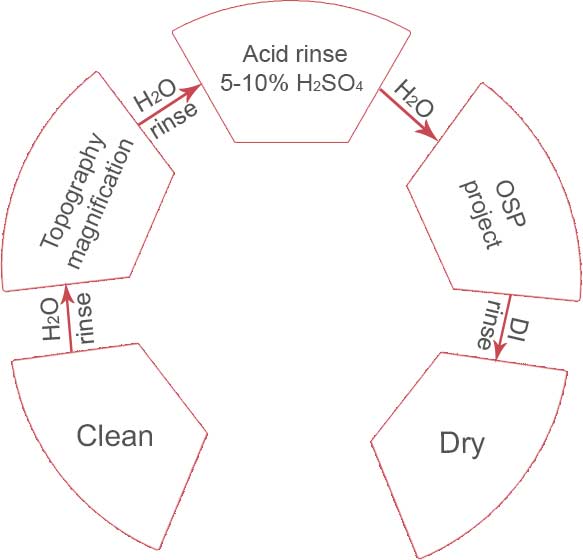
The manufacturing process for OSP is straightforward as seen in the image above. “Clean” is the starting point with cleaning off organic contaminants such as oil or fingerprints, to not get the copper foil surface contaminated before application. For the best results and performance, the cleaning process should be checked as often as possible. If it does not maintain the standards for cleanliness the performance of the application will be negatively affected.
For Topography enhancement, micro etching is applied to eliminate the oxidation generated on top of the copper foil. This is necessary for the bonding forces to be improved between the copper foil and the OSP solution. Speed is also a very important factor. In order to obtain a smooth and even film, the stability of the micro etching speed needs to be at a level of 1.0?m to 1.5?m per minute.
In the DI rinse stage after the OSP application, preservatives need to be added in order to protect the OSP solution from being polluted by other ions. If the OSP solution is polluted, tarnishing will occur soon after the reflow soldering stage. It is best that DI rinse should be utilized with preservatives that have a PH value between 4.0 and 7.0.
Handling & Controls
This surface finish is very simple and easy to control. It also has an advantage over traditional HASL with regards to coplanarity, and its solderability. However, this finish does require significant changes with the type of flux and number of heat cycles used during assembly process.
Regarding handling of this particular surface finish, there are some definite differences. You cannot touch it with your hands unprotected. Acidic fingerprints will degrade the OSP and leave the copper susceptible to oxidation. Most assemblers prefer to work with metal finishes that are more flexible and endure more heat cycles
We compiled a list of some of the advantages and disadvantages of the OSP surface finish below:
Advantages:
- Flat Surface
- Simple Process, Very Smooth Surface, Lead-Free Soldering and SMT
- Re-workable, Suitable for a Horizontal Production Line
- Cost Effective
- Environmentally Friendly
Disadvantages:
- Thickness cannot be measured
- Not Good for PTH (Plated Through Holes)
- Short Shelf Life
- Can Cause ICT Issues
- Exposed Cu on Final Assembly
- Sensitive Handling
- Cannot be Welded (reworked) more than twice
- Not Suitable for Crimping Technology & Line Binding
- Not Convenient for Visual Inspection and Electrical Measurement
- Requires Nitrogen Oxide Infused SMT
| OSP (Organic Solderability Preservatives) | ||
| PROS | CONS | MOST COMMON USES |
| Lead-FreeFlat SurfaceSimple ProcessRepairableExcellent CoplanarityImproved SolderabilityNo ‘Black Pad’ IssuesLow CostCan Be Wire Bonded | Not Good for PTHSensitive HandlingShort Shelf lifeBig Changes to Assembly ProcessICT Fixture Probes Can Potentially Damage the PCB | Copper Pad Applications |
Properties of OSP
| Properties | OSP |
|---|---|
| Contact Applications | No |
| Deposit | Dipped |
| Exposed Copper | Yes |
| Handling | Critical |
| Process Control | Fair |
| Process Cost | Poor/Fair |
| Required Thermal Cycles | ~2 |
| Shelf Life | Medium (9-12 Months)* |
| SMT | Flat |
| Thickness | 8 – 24 µin |
| Thin Board Finish | Yes |
*Requires Unique Storage Techniques µin = Microinches
Applications of OSP
| Applications | OSP |
|---|---|
| BGA & ?BGA | Yes |
| Contact/Connector | No |
| Fine Pitch SMT | Yes |
| Flip Chip | Yes |
| High Reliability | Medium/High |
| RoHS Compliant | Yes |
| Solder Joint Integrity | Good |
| Wire Bonding | No |
OSP (Organic Solderability Preservatives) is the go-to surface finish for copper pad applications. It is a very specific surface finish and as you can see has several cons associated with it. But for the most part, OSP is a great choice for an organic solution for your surface finish.
Connect With us to Discuss Your PCB Surface Finish Needs
If you are looking for the right surface finish for your PCB assembly, we would love to have a conversation with you. San Francisco Circuits is your partner for all your PCB needs. We are flexible and dependable for your most complicated requests and needs!
We are experts in PCB surface finishes. Call us for help in choosing the right surface finish for your PCB assembly process: 800.SFC.5143 or chat with one of our expert staff members.
San Francisco Circuits Offers the Following Lead-Free PCB Surface Finishes
These are the lead-free PCB surface finishes we have available for your PCB order.
For more information, please contact our experts at+86 133 9241 2348 or get a PCB production quote.
| Gold Finish | May be Electrolytic Electroless, or Immersion |
| – ENIG (Electroless Nickel Immersion Gold) | 2-5 micro inches. Purpose: To prevent oxidation, extend shelf life, provide a wire bonding surface (when aluminum wire is used), and used to provide an electrically conductive surface on PCBs. Used for solderability when the flatness of the pad is critical. ENIG has shelf life longer then 12 months. |
| – Hard Gold | Purpose: “Wear and tear” used for Gold Fingers (minimum 30 micro inches),contacts, keypads soldering (maximum 17 micro inches), to prevent oxidation and extend shelf life. |
| – Soft Gold | Purpose: Used for wire bonding (Ultrasonic minimum 2 micro inches/Thermasonic minimum 30 micro inches) and to prevent oxidation and extend shelf life. |
| Immersion Silver | Use for solderability purposes (2-10 micro inches). Used for solderability when the flatness of the pad is critical. |
| Lead Free Solder | Use for solderability purposes (70-200 micro inches). Used for solderability when the flatness of the pad is not critical. |
| OSP Organic Solderability Preservatives) | Used for solderability when the flatness of the pad is critical. |
| White Tin (Immersion Tin) | Used for solderability when the flatness of the pad is critical. |
We Can Help You Choose the Right Surface Finish For Your Applications
San Francisco Circuits specializes in helping you choose the right PCB surface finish. You have a lot of factors to think about like cost, application environment, lead/lead free requirements, shelf life, and so much more! Let us worry about those things and give you the right PCB surface finish.
When it comes to choosing the right type of surface finish, you want to make sure you select the best one for end performance. That’s where you can work with our trusted engineers who have the experience you need to get what’s best for your situation. We look forward to connecting with you!
Submit a quote for your specific PCB surface finish requirements or Contact us freely if has any need. Our email address: [email protected] . Skype ID: [email protected] . WhatsApp: +8613392412348. And our sales and engineer team will response to you once receive your quotation!