The backdrill process removes stubs from plated-through-holes (vias). Stubs are the unnecessary / unused portions of vias, which extend further than the last connected inner layer.
Stubs can lead to reflections, as well as disturbances of capacity, inductivity and impedance. This discontinuity errors become critical with increasing propagation speed.
Backplanes and thick Printed Circuit Boards in particular, can endure significant signal integrity disturbances through stubs. For High Frequency PCBs (e.g. with Impedance control), the application of backdrilling, as well as the application of blind and buried vias, can be part of the solution.
Backdrill can be applied to any type of circuit board where stubs cause signal integrity degradation, with minimal design and layout considerations. In contrast, when using blind vias, the aspect ratio has to be kept in mind.
Advantages of Backdrill:
- Reduced deterministic jitter
- Lower bit error rate (BER)
- Less signal attenuation with improved impedance matching
- Increased channel bandwidth
- Increased data rates
- Reduced EMI radiation from the stubs
- Reduced excitation of resonance modes
- Reduced via-to-via crosstalk
- Aspect ratio can be neglected (in contrast to blind vias)
Design Parameters
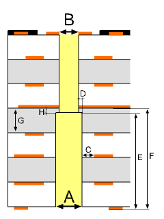
| Index | Type | Value min. |
|---|---|---|
| A | Backdrill Ø | 400µm |
| B | Plated-through via Ø | 200µm |
| C | Copper clearance | 150µm |
| D | Ø-Difference circumf. | 100µm |
| E | Backdrill depth | 200µm |
| F | Distance to connected layer | see below |
| G | Thickness target layer | see below |
| H | Thickness stub remainder (safety) | see below |
Required target layer thickness “G”
If you need a special layer buildup, please keep to the following min. prepreg thickness of the layer in which the drilling stops (G).
If you do not need a special layer buildup, we will do all the necessary thickness calculations regarding the thickness of “G”.
| F ≤ 1.0mm | 1.0mm < F ≤ 2.0mm | 2.0mm < F ≤ 3.0mm | 3.0mm < F ≤ 4.0mm | |
|---|---|---|---|---|
| G min. | 250µm | 300µm | 400µm | 500µm |
| H | 125µm | 150µm | 200µm | 250µm |
| Tolerance | ± 100µm | ± 125µm | ± 175µm | ± 225µm |
Submit a quote for your specific PCB Backdrill technology requirements or Contact us if you would like to arrange a tour of our production facility. Our email address: [email protected] . Skype ID: [email protected] . WhatsApp: +8613392412348. And our sales and engineer team will response to you once receive your quotation!