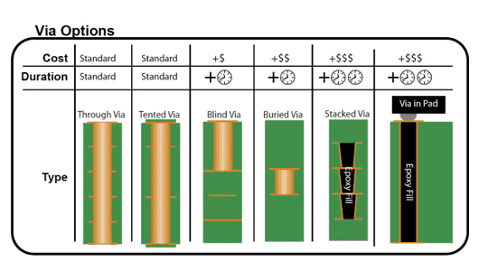
With the development of electronic products and applications of finer pitch devices, vias play an important role in the interconnection between layers in a PCB, there are three main types of vias: through hole vias, blind vias and buried vias, each of them have different attributes and functions contributing to the overall optimal performance of circuit boards or even electronic products. However, via in pad have been widely used in small-scale PCBs and BGA. With the necessity of high-density BGAs (ball grid arrays) and the miniaturization of SMD chips, the use of via in pad technology is increasingly important.
What is via in pad?
When it comes to PCB design or PCB fabrication, via in pad is a printed circuit board design technology to increase PCB density, allowing higher PCB component density (particularly in SMT IC and BGA area). what’s more, via in pad, which the annular ring of via is exposing with HAL( such as the components pad exposes), it is without any treatment in PCB fabrication. However now via in pad is more and more normal with BGA packages are becoming tighter. And not using the standard “dog bone” land pattern to transfer signal from the BGA footprint to a via that passes signal to other layers, vias can be drilled directly into the BGA footprint pads. This allows much simpler routing by soldering directly over the via. Make sure this process is called out in your fab notes. Via in pad is usually used for testing the signal, but it’s easy to result in the short.
The advantages of via in pad
There are a lot of advantages of via in pad PCB. First of all, It’s good for increasing density, using finer pitch packages, as well as lessening inductance. What’s more, in the process of via in pad, a via is directly placed below the contact pads of the device, which can achieve greater part density and superior routing. So it can save a great quantity PCB spaces with via in pad for PCB designer.
Compared with blind vias and buried vias, there are many advantages for via in pad as follows:
Apply to fine pitch BGA;
Lead to higher density PCBs and promote space saving;
Improve thermal dissipation;
Provide a flat and coplanar surface with component attachment;
Lower inductance due to no dog-bone pads with traces;
Increase voltage capability of the via;
However, you need to confirm that your PCB manufacturer is well-equipped to fabricate your PCBs because it may cost more. If you are not able to place via in pad, putting directly and using more than one can assist in decreasing inductance.
When should I use via in pad?
It will lead to design rule check errors because of trace width, annular ring, as well as size limitations while trying to route and escape component packages with sub 0.5mm pitch with traditional routing methods. For the small pitch components, only to route them with capped via in pad can it make the circuit board routing to be as compact as possible.
And it can simplify routing for complex BGA and LGA packages as well with capped via in pad. And the components like bypass capacitors to be placed as close as possible with minimizing the surface routing so that minimizing parasitic inductance. In addition, the paths to power and grounds planes are short, which will be good for minimizing EMF emissions of high frequency designs.
Vias in thermal pads also can play an effect on heat management. In general, high power surface mount parts have a thermal pad that mounts to the circuit board. So you’d better drop vias through the board to the other side of PCB to increase the copper area for heat release.
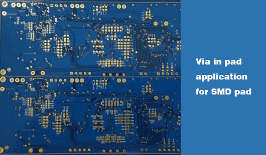
Via in pad application for SMD pad
1. Plug the via by resin and plated it flat by copper
It is compliant with small BGA via in pad;
First of all, the process is filling the via hole with a conductive or non-conductive material, and then plating the via on the surface, which provide a smooth flat for solderable surface;
There are used in via in pad designs where it can mount the component over the via, or extend the solder joint to the via connection.
2. Microvias and via in pad plated over
A microvia is a hole with a diameter of less than 0.15mm based on IPC. It can be a through via hole ( related to a aspect ratio ), however, in normal the microvia is regarded as blind vias between 2 layers;
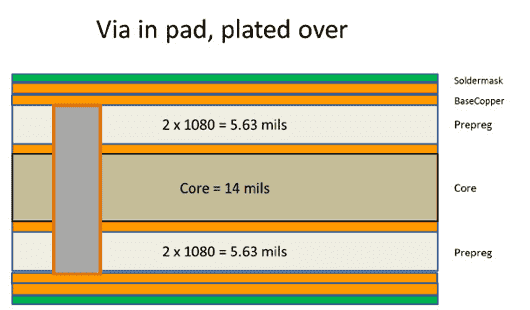
There are a majority of drilling the microvias with laser but some PCB manufacturers are also drilling them with a mechanical drill bit, which is slower, however the holes have a clean and nice cut;
The microvia cooper fill process is an electrochemical deposition process used for the multilayer PCB fabrication process, it also known as capped vias;
Although the process is complicated, it can fabricate HDI PCB that most PCB manufacturers will get the copper filling of microvias.
3. Plug the via by solder mask
It’s free and compliant with big solder SMD pads;
The standardized LPI solder mask process can not form the fill vias without the risk of exposed copper in the hole barrel. In general, it can deposit UV or thermally curable epoxy solder mask into the holes to plug them after using the second screen print;
It is known as via plugging. Via plugging is used to plug via holes with a solerrsist material so that protect air from leaking as testing the boards, or prevent the components near the board surface from shorting.
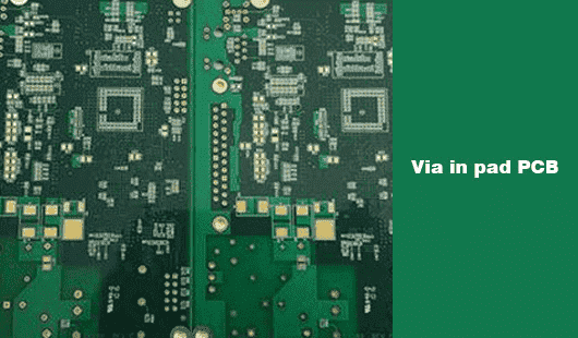
Via in pad PCB
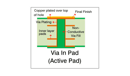
In PCB design, via is a pad with a small plated hole in a printed circuit board which are used for a connection between copper tracks on a various layers of a board. There is a via known as micro vias, which have apparent blind vias only on a single surface for high density multilayer PCB or invisible buried vias on either of the surface. What’s more, there is a new challenge after bringing in and being widely used the high density pin out parts, as well as the need for small dimension PCB. So the better solution to meet the kind of challenges is using the latest but popular PCB manufacturing technology called “ via in pad”.
It needs to quickly use via in pad in the current PCB design due to the constantly reducing pitch of part footprints, as well as the need for miniaturizing PCB form factor. What’s more, it can achieve signal routing in as little an area of the PCB layout as possible, in most instances, even avoiding escaping the perimeter of the device footprint.
Via in pads is mostly useful in high speed designs as they reduce trace length and consequently inductance. You’d better check whether your PCB manufacturer is well equipped to fabricate your board or not, because it may spend more money on it. However, if you can’t place via in pad, directly putting and using over one to decrease inductance.
What’s more, via in pad is also available in inadequate spaces such as in micro-BGA designs, and it can not use the traditional fan-out methods. Needless to say, there is less disadvantage for via in pad, because of the application of via in pad, it makes a great effect on cost. Increasing the complication of fabrication process and basic material price for conductive fill are the two primary cost factors connected with via in pad technology. Above all, via in pad is a step that add to PCB fabrication process. However, the decline in number of layers make an effect on the extra charges related to the process with via in pad technology.