As PCB signal switching speeds increase today’s PCB designer needs to understand and control the impedance of PCB traces. With the short signal transition times and high clock rates of modern digital circuitry, PCB traces need to be considered not as simple connections but as transmission lines. This simple introduction is aimed at lines running from a few hundred MHz to around 2 to 3GHz where reflections are the main concern. For higher frequencies 3GHz and upwards both this introduction – and AP8196 What is insertion loss? adds a higher frequency perspective to this easy to understand background information.
What is controlled impedance?
Probably the most common example of a controlled impedance component is the downlead (or feeder) connecting a receiving aerial to a wireless or television set. Aerial feeder leads usually take the form of “flat twin” cable (commonly supplied with VHF broadcast receivers) or low-loss coaxial cable. In both cases the impedance of the feeder is controlled by the physical dimensions and material of the cable.
PCB trace configurations
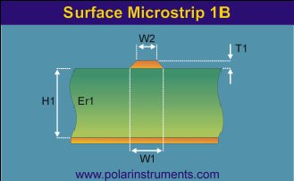
You can think of PCB traces as short cables, precisely constructed, connecting the devices mounted on the board, where the PCB trace, like the coax inner conductor, carries the signal and is insulated from its return path (in this case a ground plane) by the board laminate. This is shown in cross section in the microstrip configuration, left.
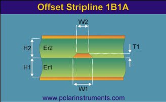
The dimensions for trace width W1 and W2, thickness T1 and laminate height H1 and H2 and the dielectric constants Er1 and Er2 must be strictly controlled. Solder resist on the surface reduces the impedance slightly so the more predictable stripline configuration shown left is often used.
So why do we need to control impedance?
The receiving aerial possesses a natural, or characteristic, impedance and electrical theory shows that for the aerial to transfer maximum power to the set (and to ensure the integrity of the electrical signal) the impedance both of the feeder and the receiver should match that of the aerial. In other words the signal should ideally be presented with a constant impedance as it travels from its source to its destination. Where a mismatch occurs only part of the signal will be transmitted; the rest will be reflected toward the source (this degrades the signal). Cable designers therefore take great care to ensure the accuracy and consistency of the cable dimensions and material characteristics. At high signal switching speeds, the electrical properties of the cable, such as the capacitance and inductance, must be taken into account, and cables can no longer be considered as simple wires. Cables designed for high signal speeds where these factors are taken into consideration are referred to as transmission lines.
Controlled impedance on PCBs
Similarly, as the speed of signal switching on a PCB increases, the electrical properties of the traces carrying signals between devices become increasingly more important. The impedance of a PCB trace is controlled by
- its configuration
- dimensions (trace width and thickness and height of the board material)
- dielectric constant of the board material
As with a cable, when the signal encounters a change of impedance arising from a change in material or geometry, part of the signal will be reflected and part transmitted. These reflections are likely to cause aberrations on the signal which may degrade circuit performance (e.g. low gain, noise and random errors). In practice board designers will specify impedance values and tolerances for board traces and rely on the PCB manufacturer to conform to the specification.
Testing the PCB
Most controlled impedance PCBs undergo 100% testing. However, it is not uncommon for the actual PCB traces to be inaccessible for testing. In addition, traces may be too short for accurate measurement and may well include branches and vias which would also make exact impedance measurements difficult. Adding extra pads and vias for test purposes would affect performance and occupy board space. PCB testing is therefore normally performed, not on the PCB itself, but on one or two test coupons integrated into the PCB panel. The coupon is of the same layer and trace construction as the main PCB and includes traces with precisely the same impedance as those on the PCB, so testing the coupon affords a high degree of confidence that the board impedances will be correct.
Measuring controlled impedance
Impedance measurements are usually made with a time domain reflectometer (TDR). The TDR applies a fast voltage step to the coupon via a controlled impedance cable and probe. Any reflections in the pulse waveform are displayed on the TDR and indicate a change in impedance value (this is known as a discontinuity). The TDR is able to indicate the location and scale of discontinuity. Using appropriate software the TDR can be made to plot a graph of the impedance over the length of the test trace on the coupon. The resulting graphical representation of the trace characteristic impedance allows previously complex measurements to be performed in a production environment.
Calculating controlled impedance
The equations for characteristic impedance require very complex mathematics, and impedances are usually calculated using field solving methods including boundary element analysis. For further details of field solving methods and Polar’s field solvers see Polar’s Si8000m multiple dielectric field solving controlled impedance design and Si9000e insertion loss GHz PCB transmission line field solver pages.
Submit a quote for your specific PCB impedance control requirements or Contact us freely if has any need. Our email address: [email protected] . Skype ID: [email protected] . WhatsApp: +8613392412348. And our sales and engineer team will response to you once receive your quotation!