We live in a world driven by technology and use them in nearly every aspect of our daily lives. We tend to depend on smart electronic devices to make our lives easier, organised and better connected. Needless to say, all these electronic devices are designed over a Printed Circuit Board (PCB). Printed circuit boards were initially developed during World War II for military applications. Over the years, this technology was adopted by electronic manufacturers enabling them to offer cost-effective, compact, and power-efficient solutions.
What is a PCB or printed circuit board?
Printed Circuit Board is a critical component in electronics that enables and integrates all the electronic circuits/components of a design. These boards are used in various electronic products — from Smartphones, Smart Tabs, Gaming Devices, Infotainment Systems to Medical devices, Industrial equipment, Automotive Electronics, Radars, Defense, Military and Aerospace equipment and all other computing systems. The printed circuit board is made up of a thin layer of conducting material, usually copper films printed over a non-conducting layer known as substrate. These substrates are made up of special materials which do not conduct electricity. The most commonly used substrates are Resins, Fiberglass, Epoxy Glass, Metal Board, Flame retardant (UL94-V0, UL94-V1) and Polyimides.
Fundamentally PCBs are single layer, double layer, and multi-layer. The layer classification of Printed Circuit Boards is based on the number of conductive layers present in the PCB. The below figure shows the cross-section of various types of PCBs.


Typically, there are two different methods for mounting components on a Printed Circuit Board — through-hole and surface-mount. In the through-hole method, the components consist of thin leads that are pressed through tiny holes in the board on one side and soldered on the other side. The through-hole method is mostly used because of the mechanical stability it provides to the components. In the surface-mount method, the terminals of every component are soldered to the same surface of the Printed Circuit Board directly. Mostly surface-mounted components are small and have a tiny set of solderable pins or Ball Grid Array (BGA) on the component.
PCB Material Classifications
A PCB is broadly classified into three different categories:
- Rigid PCB
- Flex PCB
- Rigid-Flex PCB
Let’s have a look at these categories in detail:
1. Rigid PCB
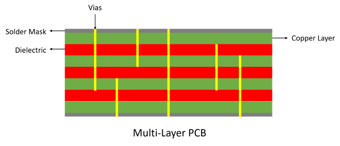
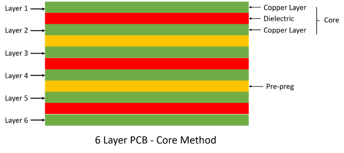
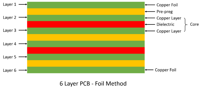
Rigid PCB, as the name suggests, is a solid, inflexible PCB which cannot be twisted or folded to fit into a specific mechanical enclosure. The Rigid PCB which is also known as the Standard PCB is made up of resin and glass along with copper foils which are generally known as Laminates. These laminates come with specific thicknesses to form a standard double-sided PCB, i.e., 0.4mm, 0.6mm, 0.8mm, 1.2mm, 1.6mm, 2.4mm, etc. Multiple sheets of these laminates are used along with pre-preg to form a multi-layer design.
Rigid PCBs are the cheapest PCBs. These are also known as the traditional PCBs and are more widely used in various electronic products. The best example of a rigid PCB is the computer motherboard. Some of the solid PCBs that we see in our daily lives are washing machine, refrigerator, telephones, and calculators.
A simple construction of the double-sided PCB and multi-layer PCB are shown below:


Benefits of Rigid Printed Circuit Boards:
- Cost-Effective solution
- Rugged and reliable
- High-density circuits
2. Flex PCB
As the name suggests, the Flex PCB is a flexible PCB that can either be folded or twisted to form a specific shape. The flexible nature of these PCBs helps in accommodating a complex PCB in a smaller form factor thereby reducing the product size. The clutters within a given frame, replacing a wires/cables with a simple flex PCB.
The substrate in the Flex PCBs is made up of thin insulating polymer films or polyimides similar to the Rigid PCBs. The key objective of Flex PCBs is to improve the bend and make the product compact and flexible with a lesser layer count. The thickness of the copper foils and the polyimides are made thinner to achieve the flexibility of the product. . “The thinner the copper foil, much reliable is the Flex PCBs.” A Stiffener/Backer is attached to the Flex PCBs to prevent plate buckling and support for components.
Ideally, Flex PCBs are a great choice for designing PCBs of high speed and controlled impedance. These PCBs are widely used in aerospace, military, mobile communications, computers, digital cameras and more.

Benefits of Flex PCBs:
- Allows bending and folding to fit into an arbitrary shape
- The thin and lightweight enables a substantial reduction in packaging size
- Flexibility makes it easier for installation and service
- Effectively reduce the volume of the product
- Suitable for miniaturized and high-reliability electronic products.
3. Rigid-Flex PCBs
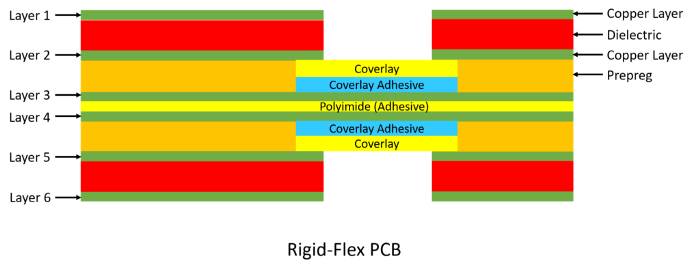
Rigid-flex PCBs are circuit boards that use a combination of both Rigid and Flexible board technologies in a given design. Typically, Rigid-Flex boards consist of multiple layers of Rigid and Flex on a PCB, that are interconnected within a 3D Space. This combination enables efficient space utilization as the flex part of the circuit can be bent or twisted to achieve the desired shape of the mechanical design.
Similar to the Rigid PCBs, standard FR4 layers merged along with polyimide layers, usually in the centre, are used to form a Rigid-Flex PCB. Rigid-Flex PCBs are most commonly found in devices were space/weight are major concerns, such as smartphones, digital cameras, USB, CT Scanners, Pacemakers, and automobiles.

Benefits of Rigid-flex PCBs:
- Rigid-Flex PCBs enable design freedom, space minimization, weight reduction, that will eventually reduce the packaging requirements significantly
- Integrates both rigid and flexible circuits to minimize interconnects
- Dynamic and flexible and fits into smaller spaces
- Suitable for high-density, miniaturized and high-reliability electronic products
- Flex circuits eliminate wire routing errors
So, there you have it. The basics of PCB and it’s classification. In the next blog, we will talk about the design and cost simplification. Till then, stay tuned!
If you have any PCB demands, please feel free to contact us.
Email:[email protected]
Skype:[email protected]
Telephone number:+86 133 9241 2348
Whatsapp: +86 133 9241 2348