HDI (High Density Interconnect PCBs)
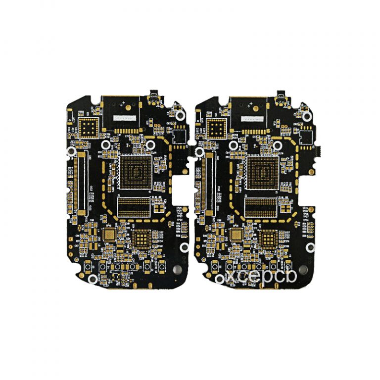
HDI PCBs (High Density Interconnect PCBs)capitalize on the latest technologies available to increase the functionality of PCBs using the same or less amount of area. This advancement in PCB technology is driven by the miniaturization of components and semiconductor packages that supports advanced features in revolutionary new products. This includes touch screen computing, 4G and 5G network communications and military applications such as avionics and smart munitions.
HDI PCBs (High Density Interconnect PCBs) are characterized by high-density attributes including laser microvias, fine lines and high performance thin materials. This increased density enables more functions per unit area. Higher technology HDI PCBs have multiple layers of copper filled stacked microvias (Advanced HDI PCBs) which creates a structure that enables even more complex interconnections. These very complex structures provide the necessary routing solutions for today’s large pin-count chips utilized in high technology products.
HDI Structures:
- 1+N+1 – PCBs contain 1 “build-up” of high-density interconnection layers.
- i+N+i (i≥2) – PCBs contain 2 or more “build-up” of high density interconnection layers. Microvias on different layers can be staggered or stacked. Copper filled stacked microvia structures are commonly seen in challenging designs.
- Any Layer HDI – All the layers of a PCB are high density interconnection layers which allows the conductors on any layer of the PCB to be interconnected freely with copper filled stacked microvia structures (“any layer via”). This provides a reliable interconnect solution for highly complex large pin-count devices, such as CPU and GPU chips utilized on handheld devices.
Advanced Capabilities: Microvias
A microvia maintains a laser drilled diameter of typically 0.006″ (150µm), 0.005″ (125µm), or 0.004″ (100µm), which are optically aligned and require a pad diameter typically 0.012″ (300µm), 0.010″ (250µm), or 0.008″ (200µm), allowing additional routing density. Microvias can be via-in-pad, offset, staggered or stacked, non-conductive filled and copper plated over the top or solid copper filled or plated. Microvias add value when routing out of fine pitch BGAs such as 0.8 mm pitch devices and below.
Additionally, microvias add value when routing out of a 0.5 mm pitch device where staggered microvias can be used, however, routing micro-BGAs such as 0.4 mm, 0.3 mm, or 0.25 mm pitch device, requires the use of Stacked MicroVias® using an inverted pyramid routing technique.
RunTek PCBs factory maintains years of experience with HDI products and was a pioneer of second generation microvias or Stacked MicroVias (SMV®). SMV® Technology offers solid copper stacked microvias providing rout-out solutions for micro BGAs.RunTek PCB factory developed and now offer an entire family of microvia technology solutions for your next generation products.
The list below shows RunTek PCB manufacturer entire family of Microvia Technology.
Standard or First Generation Microvias
- Create routing density (eliminate through vias)
- Reduce layer count
- Enhance electrical characteristics
- Standard Microvias limited to layers 1 – 2 & 1 – 3
Stacked MicroVias (SMV®) or Second Generation Microvias
- Allows increased routing on multiple layers
- Provides routing solutions for next generation applications
- 1 mm – 0.8 mm – 0.65 mm – 0.5 mm – 0.4 mm – 0.3 mm & 0.25 mm
- Provides solid copper plate eliminating potential solder voiding
- Provides a Thermal Management Solution
- Improves Current Carrying Capability
- Improves Current Carrying Capability
- Provides a Planar surface for BGA (Via-in-Pad)
- Allows any layer via technology
Deep Microvias (DpMV™)
- Provide additional dielectric material & small geometry features.
- Improved Impedance performance
- Provides RF Microvia solutions
- Provides a solid copper plate
- Improves Current Carrying Capability & Thermal Management
- Provides a Planar surface for BGA (Via-in-Pad)
Deep Stacked MicroVias (DpSMV™)
- Provides additional dielectric for RF applications
- Maintains small geometries on multiple layers
- Improved signal integrity
- Provides a solid copper plate
- Improves Current Carrying Capability & Thermal Management
- Provides a Planar surface for BGA (Via-in-Pad)
Any layer HDI (High Density Interconnect PCBs)
- Multilayer copper filled stacked micro via structure
- 1.2/1.2 mil line/space
- 4/8 mil laser via capture pad size
- Material options:
- High temperature FR4
- Halogen – Free
- High Speed (low loss)
NextGen-SMV Technology (This is a sub category to HDI)
RunTek Tech developed and now offers third generation microvias or NextGen-SMV® which offers stacked microvia fabrication in a timely manner (5-7 days). NextGen-SMV® Technology allows for a quick-turn of PCB designs with complex via structures and requires only one lamination cycle reducing thermal excursions (thermal degrading of material) and cycle time.
NextGen-SMV® eliminates the copper plating cycle of inner layers, improving impedance tolerance, reducing overall thickness and improving electrical characteristics. Additionally, NextGen-SMV® provides designer flexibility to have any-layer-via connectivity using a metallurgical bond between conductive paste and copper on the inner layers. SMV® Technology can also be utilized with NextGen-SMV for the surface or external microvias to create a solid copper via if required.
Additionally, NextGen Sub-Link Technology® allows interconnecting of multiple subs containing high technology or standard technology. Also, this technology allows the use of high performance materials only where they are needed or required.
Any HDI Board(High Density Interconnect PCBs) projects need production please send email to us: [email protected] . RunTek PCBs factory is no doubt your best PCB manufacturer choice!RunTek PCBs factory with low cost and high quality PCB products, excellent service!

