In a general sense, transmission lines are electrical transmission lines connecting the power supply of kilos of volts from the thermal generating station to distributors and consumers. However, there also exist transmission lines, which carry electricity of lower voltage and higher frequencies.
PCB Transmission Lines:
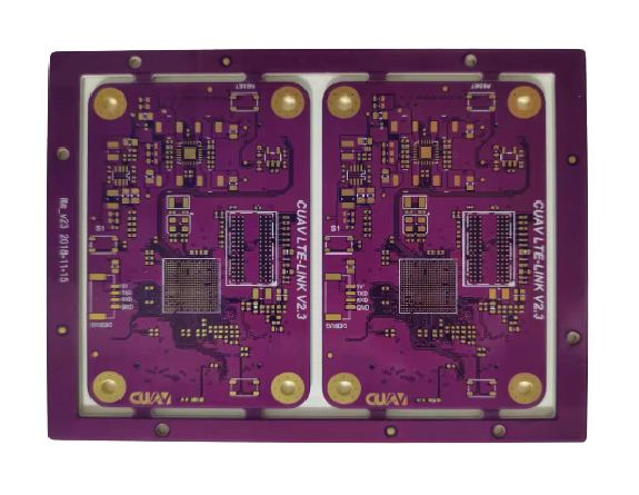
A PCB transmission line connects moving signals from their transmitters to their receivers on a printed circuit board (PCB). It has two main components — a signal trace and a return path for the ground, typically a ground plane. The space between the two components, more precisely conductors, is made up of the PCB dielectric material.
At higher frequencies, the physical scope of PCB traces becomes significantly relative to the wavelength of the signal. The facet of circuit design and analysis changes vividly as frequency increases. RF signals do not travel along wires or PCB traces straightforwardly, as we expect in low-frequency circuits.
Which one is the transmission line and which is not?
If the frequency of the signals traveling on an electric wire is low enough, it can be assumed that the wire’s voltage at a given time is the same throughout the length of the wire, then Transmission lines are not necessary. However, if the frequency of the traveling signal is very high and at the same time the length of the interconnect PCB trace is large, then this is the place to use transmission lines instead of just an ordinary interconnect.
An interconnect is considered a transmission line when its length is at least one-fourth of the signal wavelength passed through it.
Types of Transmission lines used in PCB:
Coaxial Line:
The first one and the simplest one is the coaxial line. A coaxial line has a circular shape. This circular cable is composed of a central wire conductor for the signal and an outer circular conductor for the return path. A dielectric material fills the space between the two conductors.
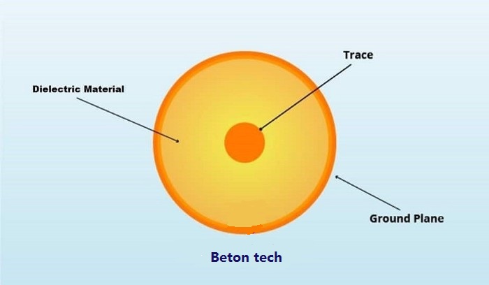
Coaxial lines are widely used as cables for high-frequency applications, such as television, music, etc.
These are non-conventional PCB transmission lines since they are non-planar. The first scenario where they are fruitful is when routing a signal through the PCB. Passing from one layer of the PCB to another is done with round pads on each layer and holes plated with metal to connect these pads. These pads are surrounded by a ground plane. Here the use of Coaxial lines is very convenient.
Next, minimal coaxial lines are available in semi-rigid form having relatively small outer diameters — as low as 0.2mm. These coaxial lines are a perfect way to provide a fully shielded path for signals on PCBs in low volume production, as rework, and for prototyping. Because of their small sizes, they tend to bend easily and be trimmed and cut according to necessity.
Microstrip Line:
A microstrip transmission line is composed of a single uniform trace to carry the signal — placed on the top layer of a PCB and parallel to a conducting ground plane, which provides the return path for the signal. The trace and the ground plane are parted by a certain height of the PCB dielectric.
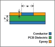
A Microstrip Transmission Line with definite Impedance is formed by a PCB Trace of appropriate geometry, Set apart from a Ground Plane. These are quite popular, maybe due to ease of fabrication & availability. With the thin layer of Epoxy or solder mask, the microstrip line becomes the Embedded microstrip line.
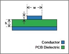
The fault observed in these lines is that some of the energy transmitted may be coupled into space or adjacent traces, resulting in loss of energy plus disruption in the adjacent traces.
Stripline:
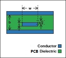
Stripline was invented by flattening the coaxial line configuration of the PCB transmission line. A stripline is composed of a uniform trace to carry the signal placed on the inner layer. The trace is separated on each side by a parallel PCB dielectric layer and then a conducting plane. So, it has two return paths. The return current path for a high-frequency signal trace is located directly above and below the ground/power planes’ signal trace. Thus, the high-frequency signal is contained entirely inside the PCB, minimizing emissions and providing natural shielding against incoming spurious signals.
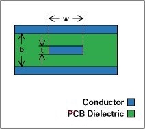
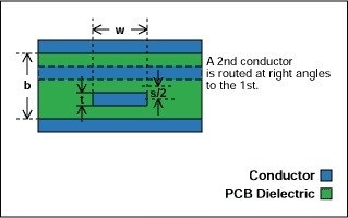
Here, again on the orientation in which the trace is placed on PCB gives rise to cantered stripline an ideal situation, off-center stripline, and the dual orthogonal stripline configuration used in high-density routing situations and is accomplished by routing two off-center layers at right angles to each other.
Coplanar Waveguide:
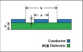
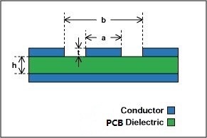
A coplanar waveguide structure has the signal trace and the return path conductor on the same layer/side of the PCB. The signal trace is at the center and is surrounded by the two adjacent outer ground planes; it is called “coplanar” because these three flat structures are on the same plane. The PCB dielectric is located underneath. Both microstrips and strip lines may have a coplanar structure.
The coplanar waveguide configurations that are used are coplanar waveguide and coplanar waveguide with the ground.
This is all about the basics of transmission lines in PCBs. These lines have an impedance at every point throughout their length, and if the line geometry is the same along the length, the line impedance is uniform. This is the case of the controlled impedance line. Non-uniform impedance causes signal reflections and distortion. It means that at high frequencies, transmission lines need to have a controlled impedance to predict the signals’ behavior.
Care should be taken to avoid the transmission line effects like signal reflections, crosstalk, electromagnetic noise, and other issues that could severely impact the signal quality and cause errors.
Layers in PCBs:
We know that the basic composition of a Printed Circuit Board (PCB) has 4 main layers, namely:
- Substrate
- Copper Foil/Sheeting
- Solder Mask
- Silkscreen
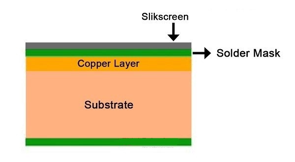
Printed circuit boards (PCBs) can consist of one layer to multiple layers. When glued into boards, these layers carry circuits that power a variety of electronic appliances. The number of layers used for a PCB depends on the application, the operating frequencies, pin density, and the requirement for signal layers and manufacturing cost with time.
Types of PCBs based on the number of Layers:
Now let us see the variety of PCBs available depending on the number of layers they are composed of (other than the fundamental layers).
Single-Layer PCBs:
Single-layer PCBs are the most primitive of their kind. Used since the 1950s, these are the PCBs found in the basic versions of Calculators, the low-priced radio alarm clocks from general supply stores, kitchen appliances such as coffeemakers, digital clocks, sensors, LED lights, printers, surveillance cameras, and timing circuits.
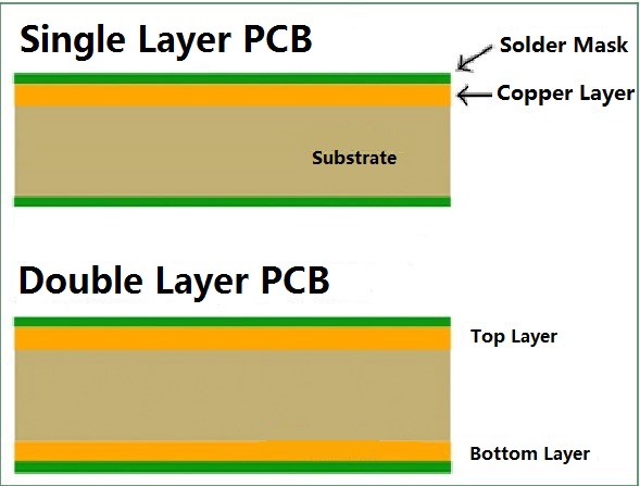
Construction-wise, the single-layer PCBs are quite simple. They consist of a thermally conductive dialectic covered first with a copper laminate and then with a solder mask.
These types of PCBs are still in use mainly because-
- They have a simple design thus easy to manufacture
- Affordable and convenient for mass production.
Double-Layer PCBs:
Double-layer PCBs are meant to support a broader range of contemporary electronics devices than one-layer PCBs. Mass-manufactured devices such as HVAC units, Amplifiers, Printers contain two-layer PCBs. They have also been used in control relays, power supplies, LED lighting, line reactors, and vending machines.
A two-layer PCB is quite a bit like the single-layer PCB, but with an inverted, mirror-image bottom half. Here, the dielectric layer is thicker than in the single layer. Additionally, the dielectric is laminated with copper on both the top and bottom sides. Moreover, the lamination is covered with a solder mask on both the top and bottom.
These allow more routing traces, since two layers. Some perks of the double layer PCBs
- The flexible, simple design thus suitable for a wide range of devices
- Fit for a range of modern-day applications
- Suitable for mass production because of its low-cost
- Small size
Four-Layer PCBs:
A four-layer PCB comprises a more complex set of layers than the one- or two-layer PCB. few crucial modern-day devices that feature four-layer PCBs are
- Many Satellite systems meant for communication across the globe make use of Multilevel PCBs.
- The high-functioning phones and tablets.
- Space probe equipment enables the study of bodies in the faraway galaxy.
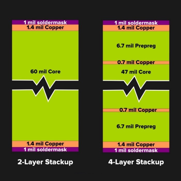
In the 4-layer PCB design, the four copper strips are divided internally by three inner dielectrics and sealed at the top and bottom by a solder mask. Four-layer PCBs are beneficial, and the following reasons prove this:
- The four-layer PCB showcase higher durability than one- and two-layer PCBs.
- Compact size and designs open doors to many applications
- These can work in both simple and complex devices
- Even with a lot of layers, they provide good safety to the user
- Since four layers are used, there is a minimum requirement for internal wiring, thus weighs less.
Six Layer PCBs:
In six-layer PCB, the circuit board technology is very much advanced than all the previous layer types. The six-layer PCB stack-up is similar to the four-layer, but with two extra copper layers and two additional dielectric material rows.
PCBs with six or more layers have allowed computer technology to grow in multi folds over the past two decades.
- If it wasn’t for the 6-layer PCBs, the evolution of computers from large CRT types to handheld ones would have been so difficult.
- There is a huge development in data storage devices, mainly due to 6-layered PCBs.
- These are also used in the Fire alarm system with the fastest and precise real-time threat detection.
- These are also used in cell phone transmission, fiber-optics receptors, heart monitors, industrial controls, and GPS technology.
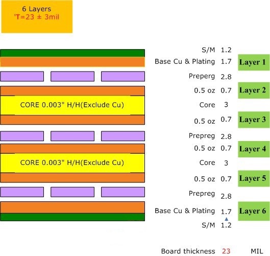
Some of the main pros of six-layer PCBs include:
- 6-layered PCBs are way more robust than any thin layered PCBs
- they have superior technological capacity thus compact fit
- provides electronic devices with optimal power and dramatically reduces the possibility of cross-talk and electromagnetic interference.
Complex Multilayer PCBs:
With the increase in the number of layers from 4 and 6, layers of conductive copper and dielectric material get added to the stack up.
Let us say an eight-layer PCB. It contains four planes and four signal copper layers — eight in all — bonded by seven inner rows of dielectric material. The eight-layer stack-up is sealed at the top and bottom with a dielectric solder mask. The eight-layer PCB stack-up is much like the six-layer, but with additional pairs of copper and prepreg columns.
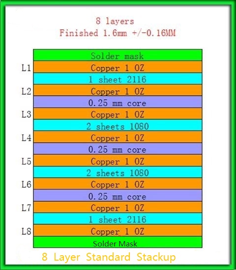
The same pattern is followed in the 10-layer PCB, which adds two more copper layers for a total of six signals and four plane copper layers, making ten layers together. Bonding the copper in the 10-layer PCB stack up are nine columns of dielectric material — five prepreg and four cores. Ten-layer PCB stacks are packed with a dielectric solder mask at the top and bottom like the rest.
At 12-layer PCB stack up, you have a board with four planes and eight conductive signal layers, bonded by six signals and five core columns of dielectric material. 12-layer PCB stacks are sealed with a dielectric solder mask.
Multilayer PCBs of the eight-, 10- and 12-layer varieties are beneficial in numerous high-tech devices and computer systems. In recent decades, the development of multilayer printed circuit boards has led to the rapid advancement from the kHz of computer systems to today’s GHz machines.
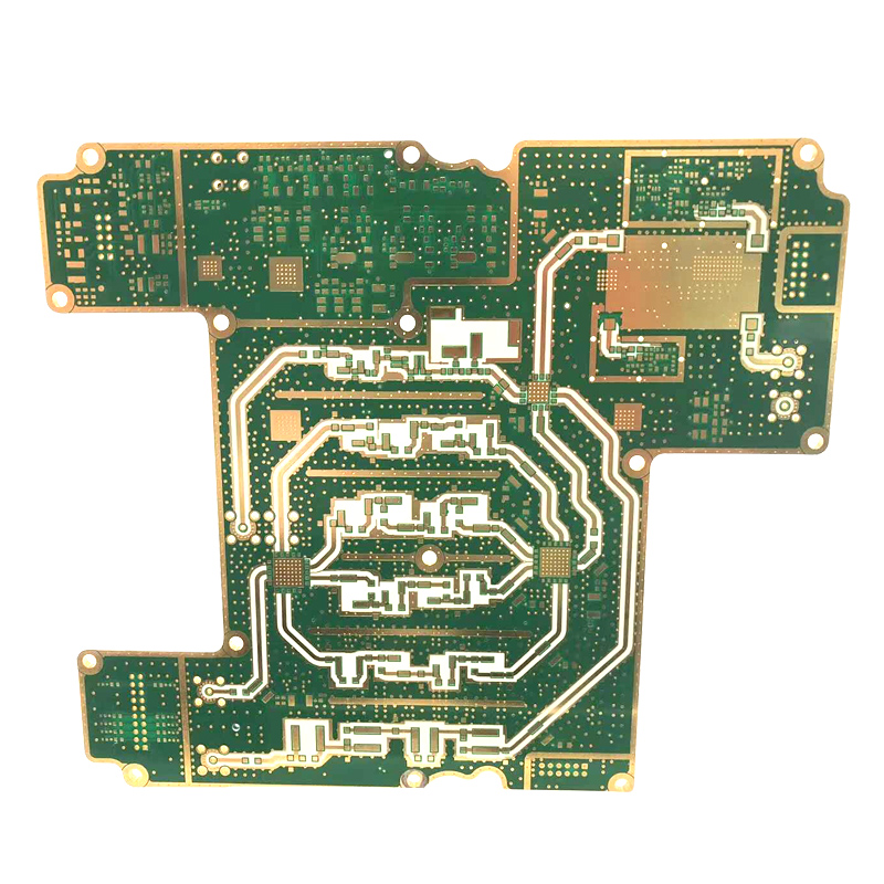
Machines and devices in a range of sectors — commercial, industrial, medical, government, aerospace — continue to grow in speed, capacity, compactness, and ease of use, thanks to the rapid developments afforded by today’s increasingly complex multilayer PCBs.
If you have any PCB demands, please feel free to contact us.
Email:[email protected]
Skype:[email protected]
Telephone number:+86 133 9241 2348
Whatsapp: +86 133 9241 2348