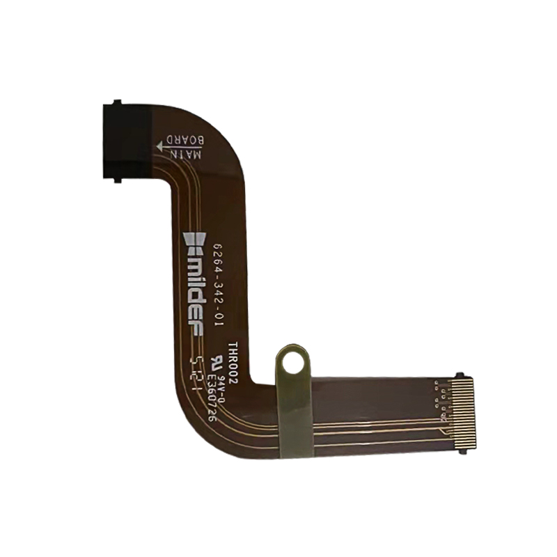
With the development of society, more and more things are becoming more and more intelligent. The premise of this is to have more circuit board SMD to control these devices, and FPC patch processing is one of the most important links. The quality of FPC SMD processing determines the life and quality of this product. The following will introduce how to check and accept FPC SMD processing products.
Acceptance criteria for FPC SMD processing products
1.Silk screen reversal
The polar dots (white silkscreen) on the component are in the same direction as the silkscreen on the PCB. (acceptable)
The polarity dots (white silkscreen) on the components do not match the diode silkscreen on the PCB board. (be rejected)
2.Too much tin
The maximum height (E) of the solder joint can extend to the top of the PAD or end cap metallization, to the solderable end, but not touching the component body. (acceptable)
Solder has touched the top of the component body. (be rejected)
3.Reverse
If the exposed electrical material is exposed, the chip component will have the opposite orientation to the material surface and the printed surface. Chip assemblies only allow inversion of one assembly ≤ 0402 per Pcs board. (acceptable)
If there is exposed electrical material, the chip component will have the same material surface as the printed surface. Chip assemblies have two or more assemblies, each Pcs board ≤ 0402. (be rejected)
4.Air welding
The solder joints between the component leads and the PAD are wet and full, and the component leads are not lifted. (acceptable)
Component leads are not coplanar, preventing acceptable soldering. (be rejected)
5.Cold welding
During the reflow process, the solder paste is fully stretched, the tin on the solder joints is completely wet, and the surface is smooth. (acceptable)
The solder paste on the solder balls was not fully reflowed, the tin was black and irregular in appearance, and the solder paste had incompletely melted tin dust. (be rejected)
6.Missing Components
The BOM list requires the patch bits to be installed but not installed. (Refuse)
The BOM list requires that the patch bit numbering does not require the component to be installed, but the component is installed and redundant parts are present anywhere. (be rejected)
7.Damage
Any edge stripping is less than 25% of the component width (W) or component thickness (T) and the top metal plating is missing up to 50% (per end). (acceptable)
Any cracks or dents exposed due to clicks, cracks or any damage in the body of the glass part, any resistance material gaps, any cracks or indentations. (be rejected)
8.Foaming, layering
The area of foaming and delamination does not exceed 25% of the spacing between plated through holes or internal lines. (acceptable)
The area of foaming and delamination exceeds 25% of the spacing between plated through holes or internal conductors, and the area of foaming and delamination reduces the spacing of the conductive patterns to a minimum electrical clearance. (be rejected)
Only by strictly implementing the acceptance procedures can the quality of FPC SMD processing products be guaranteed. Only by paying more attention to quality can we survive in an increasingly competitive market.
If you have any PCB demands, please feel free to contact us.
Email:[email protected]
Skype:[email protected]
Telephone number:+86 133 9241 2348
Whatsapp: +86 133 9241 2348