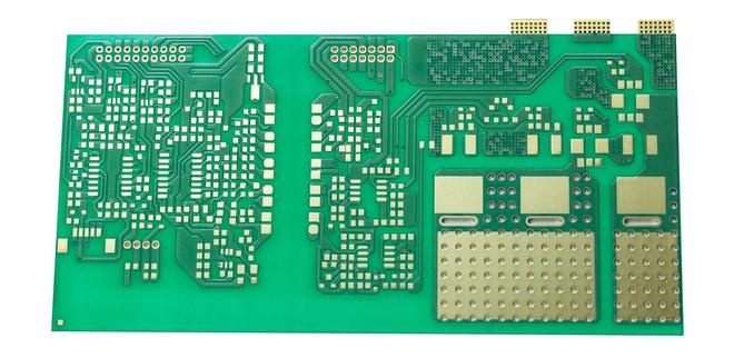
In the production process of ceramic PCB circuit board processing, laser processing mainly includes laser drilling and laser cutting.
Ceramic materials such as alumina and aluminum nitride have the advantages of high thermal conductivity, high insulation and high temperature resistance, and are widely used in the fields of electronics and semiconductors. However, ceramic materials have high hardness and brittleness, and their forming and processing are very difficult, especially the processing of micropores. Due to the high power density and good directionality of the laser, at present, lasers are generally used for perforating ceramic sheets. Laser ceramic perforation generally uses pulsed lasers or quasi-continuous lasers (fiber lasers). The laser beam is focused by an optical system at On the workpiece placed perpendicular to the laser axis, a laser beam with high energy density (105-109w/cm2) is emitted to melt and vaporize the material, and an airflow coaxial with the beam is ejected from the laser cutting head, and the molten material is The bottom of the cut is blown out to gradually form a through hole.
Since electronic devices and semiconductor components have the characteristics of small size and high density, the precision and speed of laser drilling are required to have higher requirements. According to the different requirements of component applications, electronic devices and semiconductor components have small size and high density. Therefore, the precision and speed of laser drilling are required to be high. According to the different requirements of component applications, the diameter of the micro-holes ranges from 0.05 to 0.2 mm. For lasers used for precision machining of ceramics, the diameter of the laser focal spot is generally less than or equal to 0.05mm. According to the thickness and size of the ceramic plate, through-hole drilling of different apertures can generally be realized by controlling the defocus amount. For through-holes with a diameter less than 0.15mm, Punching can be achieved by controlling the amount of defocus.
There are two main types of ceramic PCB circuit board cutting: water jet cutting and laser cutting. At present, most laser cutting options on the market are fiber lasers. Fiber laser cutting ceramic circuit boards has the following advantages:
(a) High precision, high speed, narrow slit, small heat affected zone, smooth cutting surface without burrs.
(b) The laser cutting head will not come into contact with the surface of the material and will not scratch the workpiece.
(c) The slit is narrow, the heat affected zone is small, the local deformation of the workpiece is extremely small, and there is no mechanical deformation.
(d) It has good processing flexibility, can process any graphics, and can also cut pipes and other special-shaped materials.
With the continuous advancement of 5G construction, industrial fields such as precision microelectronics and aviation and ships have been further developed, and these fields all cover the application of ceramic substrates. Among them, ceramic substrate PCB has gradually been used more and more because of its superior performance.
Ceramic substrate is the basic material of high-power electronic circuit structure technology and interconnection technology, with dense structure and certain brittleness. In the traditional processing method, there is stress in the drilling process, and it is easy to crack for the thin ceramic sheet.
Under the development trend of thinning and miniaturization, the traditional cutting method can no longer meet the demand because the precision is not high enough. Laser is a non-contact processing tool, which has obvious advantages over traditional processing methods in cutting technology, and plays a very important role in PCB processing of ceramic substrates.
With the continuous development of the microelectronics industry, electronic components are gradually developing in the direction of miniaturization and thinning, and the requirements for precision are getting higher and higher, which is bound to put forward higher and higher requirements for the processing degree of ceramic substrates. From the perspective of development trends, the application of laser processing ceramic PCB substrates has broad prospects for development!