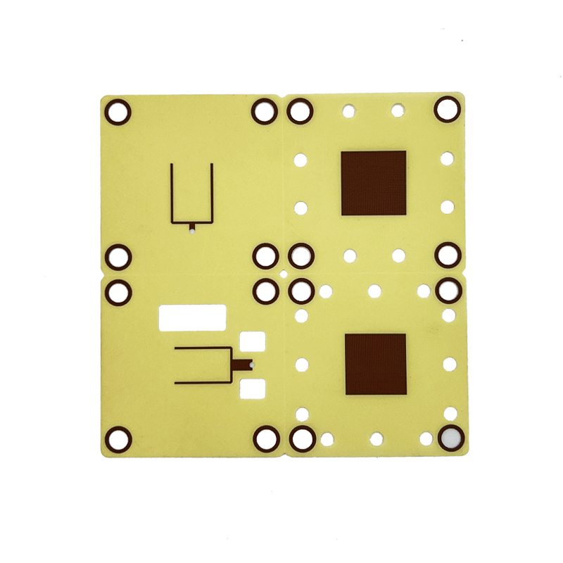
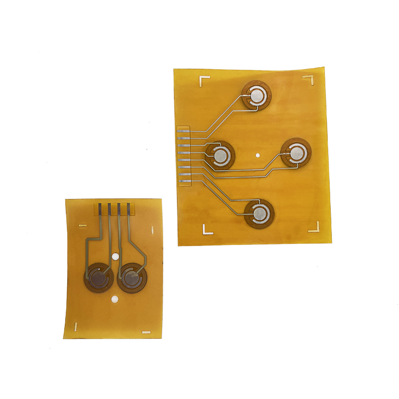
1. Flexible circuit board FPC plating
(1) Pretreatment of FPC electroplating The surface of the copper conductor exposed by the FPC coating process may be contaminated by adhesive or ink, as well as oxidation and discoloration caused by the high temperature process. A tight coating with good adhesion must remove the contamination and oxide layer on the conductor surface and make the conductor surface clean.
However, some of these contaminations are very firmly combined with copper conductors, and cannot be completely removed with weak cleaning agents. Therefore, most of them are often treated with alkaline abrasives with a certain strength and polishing brushes. Most of the coating adhesives are ring-shaped. Oxygen resins have poor alkali resistance, which will lead to a decrease in bonding strength. Although it is not obvious, in the FPC electroplating process, the plating solution may infiltrate from the edge of the cover layer, and in severe cases, the cover layer will be peeled off. . The phenomenon of solder drilling under the overlay occurs during final soldering. It can be said that the pre-treatment cleaning process will have a significant impact on the basic characteristics of the flexible printed board, and full attention must be paid to the processing conditions.
(2) Thickness of FPC electroplating When electroplating, the deposition speed of the electroplated metal is directly related to the electric field intensity, and the electric field intensity changes with the shape of the circuit pattern and the positional relationship of the electrodes. The sharper the point, the closer the distance to the electrode, the greater the electric field strength, and the thicker the coating at that part. In applications related to flexible printed boards, there are many cases where the width of many wires in the same circuit is very different, which makes it easier to produce uneven thickness of the coating. In order to prevent this from happening, a shunt cathode pattern can be attached around the circuit. , absorb the uneven current distributed on the electroplating pattern, and ensure that the thickness of the coating on all parts is uniform to the greatest extent.
(3) Therefore, efforts must be made in the structure of the electrodes. A compromise solution is proposed here. The standards for the parts with high requirements on the uniformity of the coating thickness are strict, and the standards for other parts are relatively relaxed, such as lead-tin plating for fusion welding, gold-plating for metal wire lap (welding), etc. High, and for general anti-corrosion lead-tin plating, the plating thickness requirements are relatively relaxed.
There is no problem with the smudges and dirt of FPC electroplating, which has just been plated, especially the appearance. However, some surface smudges, dirt, discoloration and other phenomena appear soon after, especially when the factory inspection was not found. What is different, but when the user checks the reception, it is found that there is an appearance problem. This is caused by insufficient drifting and residual plating solution on the surface of the plating layer, which slowly undergoes a chemical reaction over a period of time. In particular, the flexible printed board is not very flat due to its softness, and various solutions are likely to “accumulate?” in its recesses, and then react in this part and change color. In order to prevent this from happening, not only should it be fully drifted, but also It should also be fully dried. It can be confirmed whether the drift is sufficient through a high temperature thermal aging test.
2. FPC electroless plating of flexible circuit boards
When the line conductor to be plated is isolated and cannot be used as an electrode, only electroless plating can be performed. Generally, the baths used in electroless plating have strong chemical effects, and the electroless gold plating process is a typical example. Electroless gold plating solution is an alkaline aqueous solution with a very high pH value. When using this electroplating process, it is easy for the plating solution to penetrate under the cover layer, especially if the quality control of the cover film lamination process is not strict and the bonding strength is low, this problem is more likely to occur.
Due to the characteristics of the plating solution, the electroless plating of the displacement reaction is more prone to the phenomenon that the plating solution penetrates into the cover layer. It is difficult to obtain ideal plating conditions by this process.
3. Flexible circuit board FPC hot air leveling
Hot air leveling is originally a technology developed for coating lead and tin on rigid printed boards. Due to the simplicity of this technology, it is also applied to flexible printed boards (FPC). Hot air leveling is to directly immerse the board in the molten lead and tin bath vertically, and the excess solder is blown away with hot air. This condition is very harsh for the flexible printed board FPC. If the flexible printed board FPC cannot be immersed in the solder without taking any measures, the flexible printed board FPC must be sandwiched between the silk screen made of titanium steel , and then immersed in the molten solder. Of course, the surface of the flexible printed board FPC must be cleaned and fluxed in advance.
Due to the harsh conditions of the hot air leveling process, it is easy for the solder to drill from the end of the cover layer to the underside of the cover layer, especially when the bonding strength between the cover layer and the surface of the copper foil is low, this phenomenon is more likely to occur frequently. Since the polyimide film is easy to absorb moisture, when the hot air leveling process is used, the moisture absorbed by the moisture will cause the cover layer to foam or even peel off due to rapid thermal evaporation. Therefore, before FPC hot air leveling, it must be dried and moisture-proof manage.
If you have any PCB demands, please feel free to contact us.
Email:[email protected]
Skype:[email protected]
Telephone number:+86 133 9241 2348
Whatsapp: +86 133 9241 2348