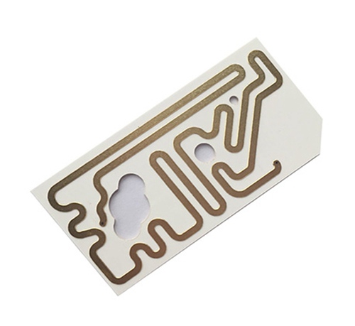
Compared with fiberglass boards, ceramic substrates are fragile. Compared with ordinary PCB boards, the process is much more difficult and requires higher process technology requirements. There are several very important process links in the production of ceramic substrates: drilling, etching, and copper coating.
Ceramic base circuit board manufacturing process-drilling
At present, ceramic-based circuit boards generally use laser perforation. The traditional LTCC and DBC technologies are gradually being replaced by DPC, and laser technology is more in line with the high-density interconnection and refinement of printed circuit boards. The ceramic circuit board through the laser drilling process has the advantages of high ceramic and metal bonding, no shedding, blistering, etc., to achieve the effect of growing together, high surface flatness, roughness of 0.1μm ~ 0.3μm, laser drilling The hole diameter is 0.15mm-0.5mm, or even 0.06mm.
The foreign laterally excited atmospheric pressure CO2 laser was developed by a Canadian company. Compared with ordinary lasers, its output power can be as high as about one hundred to one thousand times, and it is easy to manufacture. In the electromagnetic spectrum, the radio frequency is in the frequency range of 105-109Hz, and the frequency emission CO2 is developed with the development of military and aerospace technology. The small and medium-power radio frequency CO2 laser has excellent modulation performance, stable power performance, and high operational reliability. Features such as long life. UV solid YAG is widely used in materials such as plastics and metals in the microelectronics component industry. Although the CO2 laser drilling process is more complicated, and the produced microporous aperture is higher than that of UV solid YAG, CO2 laser has the advantages of higher efficiency and faster speed in drilling, and it can account for 80% of the market share in PCB laser micro-hole processing.
At present, my country’s laser drilling technology has accumulated experience and technological progress. Compared with traditional drilling technology, laser drilling technology has high accuracy, fast speed, high efficiency, large-scale batch drilling, suitable for most hard and soft materials, no loss of tools, and waste generated. The advantages of less materials, environmental protection and pollution-free.
Ceramic base circuit board manufacturing process-copper clad
Copper-clad refers to cover the area without wiring on the circuit board with copper foil and connect it to the ground wire to increase the area of the ground wire, reduce the loop area, reduce the voltage drop, and improve the power efficiency and anti-interference ability. In addition to reducing the impedance of the ground wire, copper coating also has the functions of reducing the loop cross-sectional area and enhancing the signal mirror loop. Therefore, the copper coating process plays a very critical role in the ceramic substrate PCB process. Incomplete, truncated mirror loops or incorrectly positioned copper layers often cause new interference and negatively affect the use of the circuit board.
RunTek Technology’s commonly used copper coating processes include DBC process and DPC process. In DPC process, electroplating process is used. Sputtering process is generally used to sequentially form an adhesion layer made of chromium or titanium on the ceramic surface and copper is used as the material. The seed layer and adhesion layer of the material can increase the adhesion strength of the metal circuit, and the copper seed layer acts as a conductive layer.
Ceramic base circuit board production process-etching
Ceramic base circuit board etching and its method
Ceramic-based circuit boards also need to be etched. The circuit pattern is pre-plated with a lead-tin anti-corrosion layer, and then the unprotected non-conductor part of the copper is chemically etched away to form a circuit. According to the different process methods, etching is divided into inner layer etching and outer layer etching. The inner layer etching uses acid etching, using wet film or dry film as the resist; the outer layer etching uses alkaline etching, using tin-lead as the resist .
1.Alkaline etching process of ceramic base circuit board
Film fading: Use the film fading solution to fade the film on the circuit board surface, exposing the unprocessed copper surface.
Etching: Use the etching solution to etch away the unnecessary bottom copper, leaving a thicker circuit. Among them, additives are used. The accelerator is used to promote the oxidation reaction and prevent the precipitation of cuprous ions; the bank protection agent is used to reduce side corrosion; the suppressor is used to suppress the dispersion of ammonia, the precipitation of copper and accelerate the oxidation reaction of corrosion of copper.
New lotion: Use ammonium monohydrate without copper ions, and use ammonium chloride solution to remove the remaining liquid on the board.
Hole: This process is only suitable for immersion gold process. It mainly removes excess palladium ions in non-plated through holes to prevent gold ions from being deposited in the gold immersion process.
Melting tin: Use nitric acid solution to remove the tin-lead layer.
2.Ceramic base circuit board acid copper chloride etching process
Development: Use the weak alkalinity of sodium carbonate to dissolve the part of the dry film that has not been irradiated by ultraviolet rays, and the part that has been irradiated is retained.
Etching: According to a certain proportion of the solution, dissolve and etch away the exposed copper surface with an acidic copper chloride etching solution.
Film fading: Dissolve the protective film on the line according to a certain proportion of the potion under a specific temperature and speed environment. Acidic copper chloride etching has the characteristics of easy control of the etching speed, high copper etching efficiency, good quality, and easy recycling of the etching solution.
Common problems and improvement methods of etching process
Endless film fading
Because the concentration of the syrup is low; the traveling speed is too fast; the nozzle clogging and other problems will cause the film to fade. Therefore, it is necessary to check the concentration of the potion, adjust the concentration of the potion to an appropriate range; adjust the speed and parameters in time; dredge the nozzle.
Board surface oxidation
Because the concentration of the potion is too high and the temperature is too high, it will cause the surface of the board to oxidize, so it is necessary to adjust the concentration and temperature of the potion in time.
Unfinished copper corrosion
Because the etching speed is too fast; the composition of the potion is different; the copper surface is contaminated; the nozzle is blocked; the temperature is low and other problems will cause the copper to be incompletely etched. Therefore, it is necessary to adjust the etching transportation speed; re-check the composition of the potion; be careful of copper surface pollution; clean the nozzle to prevent clogging; adjust the temperature, etc.
Copper corrosion is too high
Because the machine running speed is too slow, the temperature is too high and other reasons will lead to the phenomenon of excessive copper corrosion, so it is necessary to take measures such as adjusting the machine speed and adjusting the temperature.
If you have any PCB demands, please feel free to contact us.
Email:[email protected]
Skype:[email protected]
Telephone number:+86 133 9241 2348
Whatsapp: +86 133 9241 2348