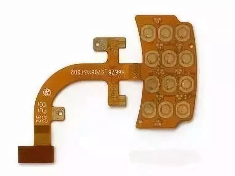
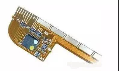
What is FPC
The flexible circuit board is a highly reliable and excellent flexible printed circuit board made of polyimide or polyester film as the base material. Referred to as flexible board or FPC.
Features: It has the characteristics of high wiring density, light weight, and thin thickness; it is mainly used in mobile phones, notebook computers, PDAs, digital cameras, LCMs and many other products.
Types of FPC
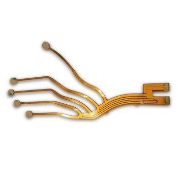
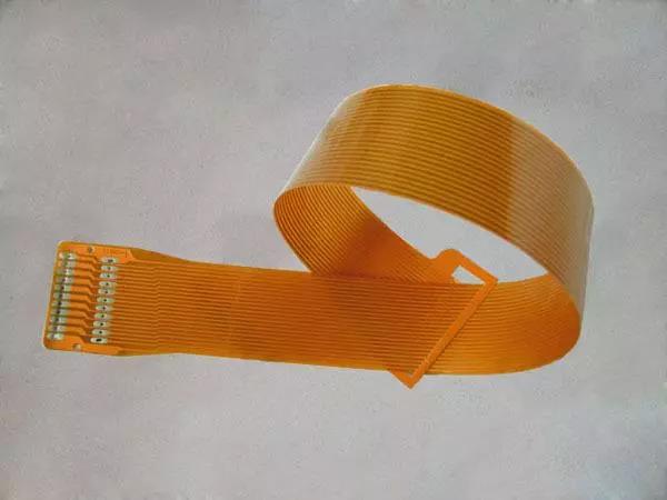
Single layer FPC
It has a layer of chemically etched conductive pattern, and the conductive pattern layer on the surface of the flexible insulating substrate is a rolled copper foil. The insulating substrate can be polyimide, polyethylene terephthalate, aramid cellulose ester and polyvinyl chloride. Single-layer FPC can be divided into the following four sub-categories:
- Single-sided connection without covering
The wire pattern is on the insulating substrate, and there is no covering layer on the wire surface. The interconnection is realized by soldering, welding or pressure welding, which is commonly used in early telephones. - Single-sided connection with overlay
Compared with the previous type, it only has an extra layer of covering on the surface of the wire. The pads need to be exposed when covering, and it can simply be left uncovered in the end area. It is the most widely used and widely used single-sided flexible PCB. It is used in automobile instruments and electronic instruments.
- Double-sided connection without covering layer
The connection pad interface can be connected on the front and back of the wire. A via hole is opened on the insulating base material at the pad. This via hole can be punched, etched or made by other mechanical methods at the required position of the insulating base material. become. - Double-sided connection with cover layer
The difference between the previous type is that there is a covering layer on the surface, and the covering layer has via holes to allow termination on both sides while still maintaining the covering layer. It is made of two layers of insulating materials and a layer of metal conductors.
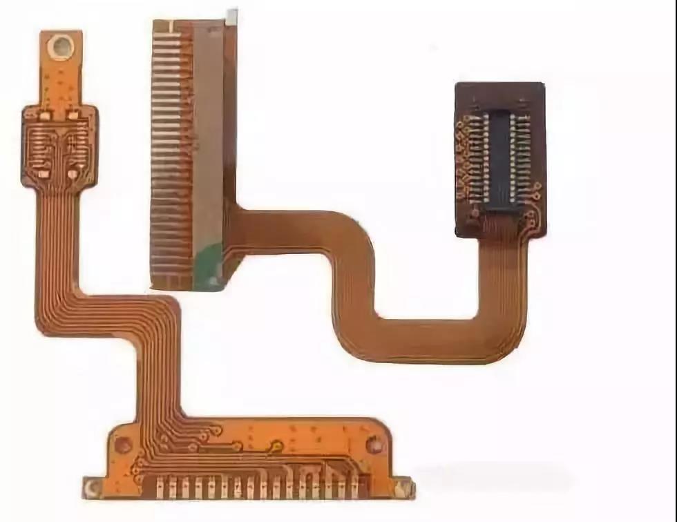
Double-sided FPC
The double-sided FPC has a conductive pattern made by etching on both sides of the insulating base film, which increases the wiring density per unit area. The metallized hole connects the patterns on both sides of the insulating material to form a conductive path to meet the design and use function of flexibility. The cover film can protect single and double-sided wires and indicate where the components are placed. According to requirements, metallized holes and covering layers are optional, and this type of FPC has fewer applications.
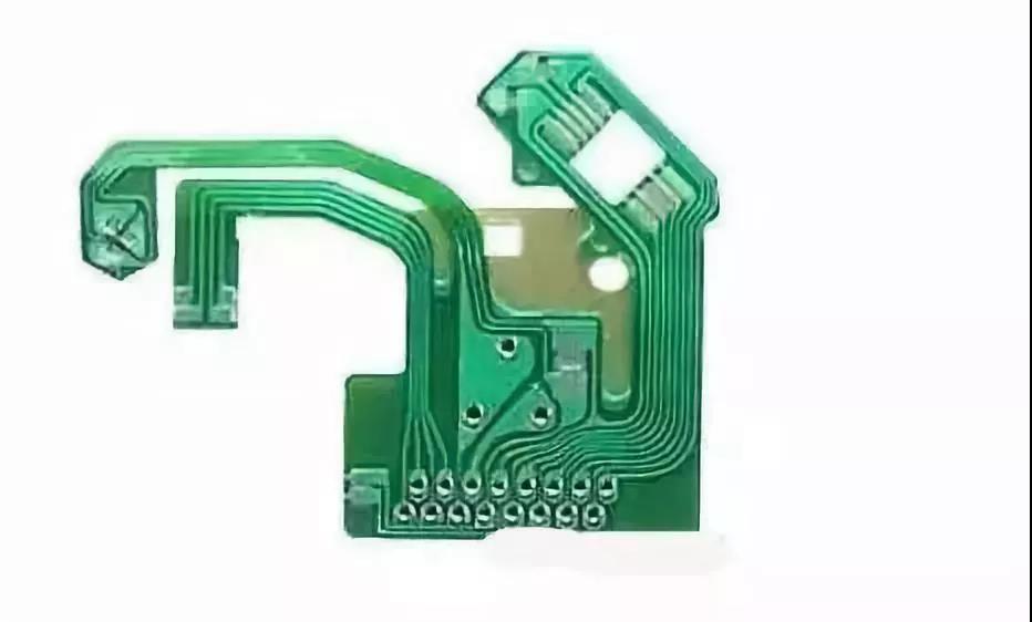
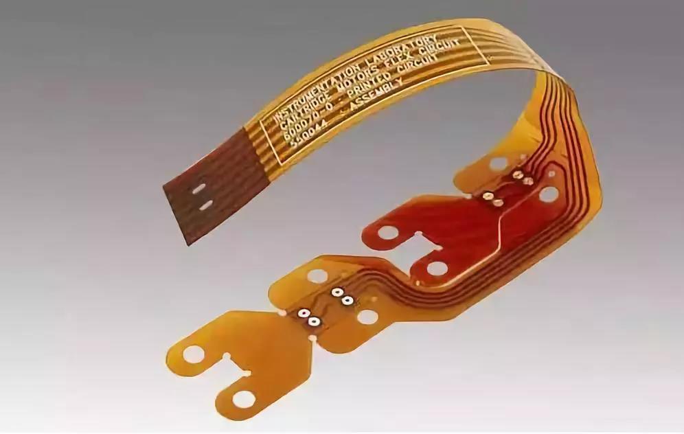
Multilayer FPC
Multi-layer FPC is to laminate 3 or more layers of single-sided or double-sided flexible circuits together, and form metallized holes by drilling and electroplating to form conductive paths between different layers. In this way, no complicated welding process is required. Multilayer circuits have huge functional differences in terms of higher reliability, better thermal conductivity and more convenient assembly performance.
The advantage is that the base film is light in weight and has excellent electrical properties, such as a low dielectric constant. The multi-layer flexible PCB board made of polyimide film as the base material is about 1/3 lighter than the rigid epoxy glass cloth multi-layer PCB board, but it loses the excellent single-sided and double-sided flexible PCB. Most of these products do not require flexibility. Multi-layer FPC can be further divided into the following types:
- Finished flexible insulating substrate
This type is manufactured on a flexible insulating substrate, and the finished product is specified to be flexible. This structure usually bonds the two-sided ends of many single-sided or double-sided microstrip flexible PCBs together, but the central parts of them are not bonded together, thus having a high degree of flexibility. In order to have a high degree of flexibility, a thin, suitable coating, such as polyimide, can be used on the wire layer instead of a thicker laminated cover layer.
- Finished soft insulating substrate
This type is manufactured on a flexible insulating substrate, and the finished product can be flexed. This type of multi-layer FPC is made of a flexible insulating material, such as polyimide film, laminated to make a multi-layer board, and loses its inherent flexibility after lamination.
FPC manufacturing process
Almost all the FPC manufacturing processes so far have been processed by the subtractive method (etching method). Usually, a copper clad board is used as a starting material, a resist layer is formed by photolithography, and the unnecessary part of the copper surface is etched and removed to form a circuit conductor. Due to problems such as undercutting, the etching method has limitations in the processing of fine circuits.
Based on the processing difficulties of the subtractive method or the difficulty in maintaining high-yield micro-circuits, the semi-additive method is considered to be an effective method, and various semi-additive methods have been proposed. Examples of micro-circuit processing using the semi-additive method. The semi-additive process uses polyimide film as a starting material. First, a liquid polyimide resin is cast (coated) on a suitable carrier to form a polyimide film.
Next, a sputtering method is used to form a seeding layer on the polyimide base film, and then a resist pattern of the reverse pattern of the circuit is formed on the seeding layer by photolithography, which is called a plating resistant layer. The blank part is electroplated to form a conductor circuit. Then remove the resist layer and unnecessary seeding layer to form the first layer of circuits. Coating photosensitive polyimide resin on the first layer of circuit, using photolithography to form holes, protective layer or insulating layer for the second layer of circuit layer, and then sputtering on it to form a seeding layer, as the second The base conductive layer of a two-layer circuit. Repeat the above process to form a multilayer circuit.
Using this semi-additive method, ultra-fine circuits with a pitch of 5um and a via hole of 10um can be processed. The key to making ultra-fine circuits using the semi-additive method is the performance of the photosensitive polyimide resin used as the insulating layer.
Composing material
Insulating film
The insulating film forms the base layer of the circuit, and the adhesive bonds the copper foil to the insulating layer. In a multi-layer design, it is then bonded to the inner layer. They are also used as a protective cover to insulate the circuit from dust and moisture and to reduce stress during flexing. The copper foil forms a conductive layer.
In some flexible circuits, rigid members formed of aluminum or stainless steel are used, which can provide dimensional stability, physical support for the placement of components and wires, and stress relief. The adhesive bonds the rigid component and the flexible circuit together. In addition, there is another material sometimes used in flexible circuits. It is an adhesive layer, which is formed by coating an adhesive on both sides of an insulating film. The adhesive layer provides environmental protection and electrical insulation functions, and can eliminate a layer of film, and has the ability to bond multiple layers with a small number of layers.
Conductor
Copper foil is suitable for use in flexible circuits. It can be electrodeposited (ED) or plated. One side of the electrodeposited copper foil has a glossy surface, while the processed surface on the other side is dull and dull. It is a flexible material that can be made into many thicknesses and widths. The matte side of ED copper foil is often specially treated to improve its bonding ability. In addition to flexibility, forged copper foil also has the characteristics of rigidity and smoothness. It is suitable for applications that require dynamic deflection.
Adhesive
In addition to bonding the insulating film to the conductive material, the adhesive can also be used as a covering layer, as a protective coating, and as a covering coating. The main difference between the two lies in the application method used. The cover layer is bonded to the cover insulating film to form a laminated circuit. Screen printing technology used for covering and coating of adhesive.

Not all laminate structures contain adhesives, and laminates without adhesives form thinner circuits and greater flexibility. Compared with the laminated structure based on adhesive, it has better thermal conductivity. Due to the thin structure of the adhesive-free flexible circuit and the elimination of the thermal resistance of the adhesive, thereby improving the thermal conductivity, it can be used in a working environment where the flexible circuit based on the adhesive laminated structure cannot be used.
Basic structure
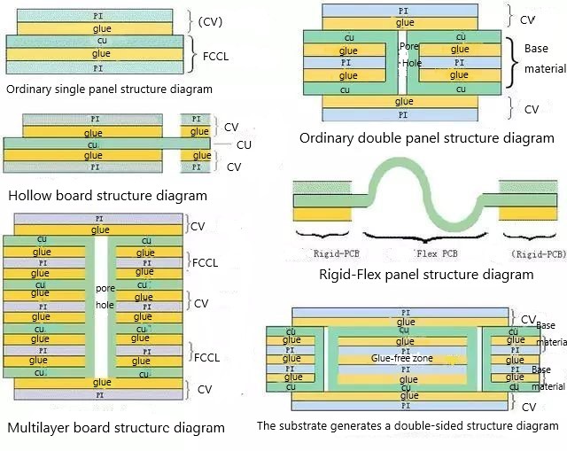
Copper foil substrate: Copper Film.
Copper foil: basically divided into electrolytic copper and rolled copper, the common thickness is 1oz, 1/2oz and 1/3oz.
Substrate film: There are two common thicknesses: 1mil and 1/2mil.
Glue: Adhesive, the thickness is determined according to customer requirements.
Covering film protection film: used for surface insulation, common thicknesses are 1 mil and 1/2 mil.
Release paper: Avoid the adhesive sticking to foreign matter before pressing, which is convenient for operation.
PI Stiffener Film: Reinforces the mechanical strength of FPC to facilitate surface mounting operations. The common thickness is 3mil to 9mil.
EMI: Electromagnetic shielding film to protect the circuit inside the circuit board from outside interference (strong electromagnetic area or susceptible to interference)
How to solder
Steps
- Before soldering, apply flux to the pad and process it with a soldering iron to avoid poor tin plating or oxidation of the pad, resulting in poor soldering, and the chip generally does not need to be processed.
- Use tweezers to carefully put the PQFP chip on the PCB board, taking care not to damage the pins. Make it aligned with the pad, and ensure that the chip is placed in the correct direction. Adjust the temperature of the soldering iron to more than 300 degrees Celsius, dip a small amount of solder on the tip of the soldering iron, press down the aligned chip with a tool, and add a small amount of solder to the two diagonal pins. Hold down the chip and solder the pins on the two diagonal positions to make the chip fixed and unable to move. After soldering the opposite corners, recheck the alignment of the chip position. If necessary, adjust or remove and realign the position on the PCB board.
- When starting to solder all the pins, add solder to the tip of the soldering iron, and apply flux to all the pins to keep the pins moist. Touch the end of each pin of the chip with the tip of the soldering iron until you see the solder flowing into the pin. When soldering, keep the tip of the soldering iron parallel to the soldered pin to prevent overlap due to excessive soldering.
- After soldering all the pins, wet all the pins with flux to clean the solder. Absorb the excess solder where needed to eliminate any short circuits and overlaps. Finally, use tweezers to check whether there is any false soldering. After the check is completed, remove the solder from the circuit board, and soak the hard brush with alcohol and wipe it carefully along the pin direction until the solder disappears.
- SMD resistor-capacitor components are relatively easy to solder. You can put tin on a solder joint first, then put one end of the component, clamp the component with tweezers, and then see if it is placed correctly after soldering one end. ; If it has been placed upright, then solder the other end.
Precautions
In the layout, when the circuit board size is too large, although the soldering is easier to control, the printed lines are long, the impedance increases, the anti-noise ability is reduced, and the cost increases; Mutual interference, such as electromagnetic interference of circuit boards.
Therefore, the PCB board design must be optimized:
- Shorten the connection between high-frequency components and reduce EMI interference.
- Components with heavy weight (such as more than 20g) should be fixed with brackets and then welded.
- Heat dissipation issues should be considered for heating components to prevent defects and rework caused by large ΔT on the surface of the components, and the thermal components should be far away from the heating source.
- The arrangement of the components is as parallel as possible, which is not only beautiful but also easy to weld, suitable for mass production. The circuit board is designed as a 4:3 rectangle.
- Do not change the wire width to avoid discontinuities in the wiring.
- When the circuit board is heated for a long time, the copper foil is easy to expand and fall off. Therefore, avoid using large-area copper foil.