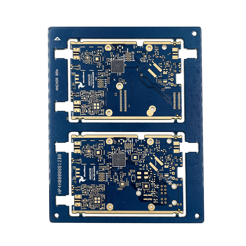
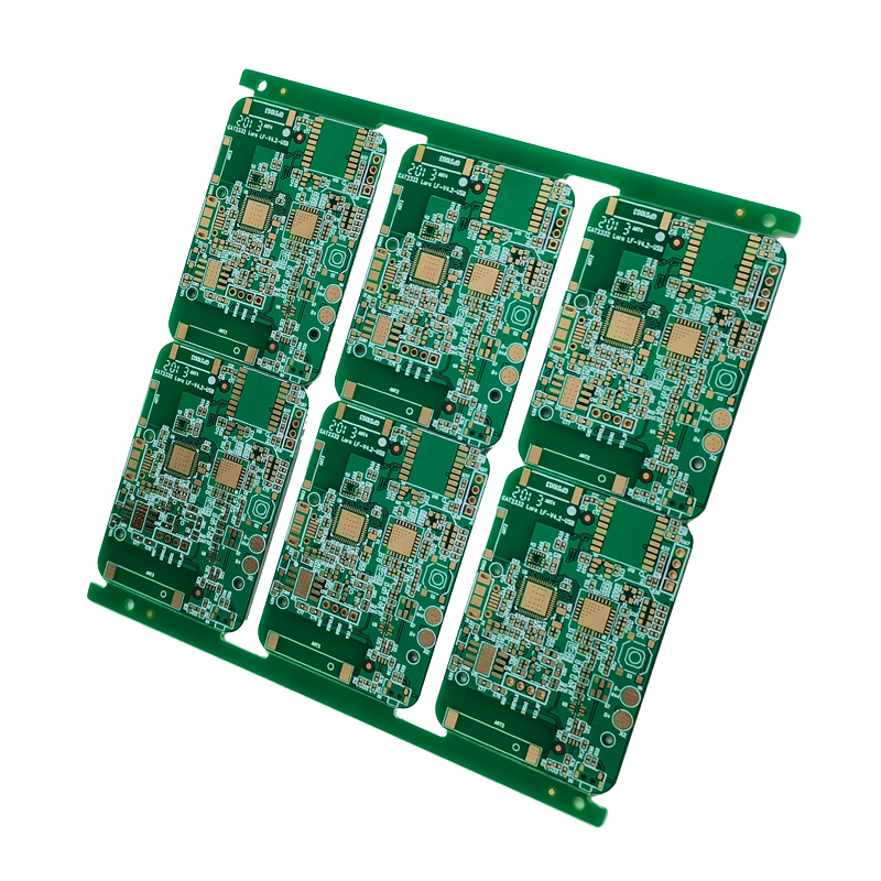
Multilayer PCB is used as the “core main force” in the fields of communication, medical treatment, industrial control, security, automobile, electric power, aviation, military industry, and computer peripherals. As the product features more and more and the circuits become more and more dense, the production difficulty becomes more and more difficult.
At present, domestic PCB manufacturers that can mass-produce high-level multi-layer circuit boards often come from foreign-funded enterprises, and only a few domestic-funded enterprises have the strength of batch production.
The production of high-level multi-layer circuit boards not only requires higher investment in technology and equipment, but also requires experienced production technicians. At the same time, the introduction of high-level multi-layer board customer certification, the procedures are strict and cumbersome. Therefore, the entry threshold for high-level multi-layer circuit boards is relatively high, and the industrialized production cycle is long.
Specifically, the processing difficulties encountered in the production of high-level circuit boards are mainly the following four aspects.
1.Difficulties in making inner-layer circuits
The multi-layer board circuit has various special requirements of high speed, thick copper, high frequency and high Tg value, and the requirements for inner layer wiring and pattern size control are getting higher and higher.For example, on the ARM development board, there are many impedance signal circuits in the inner layer. To ensure the integrity of the impedance increases the difficulty of the inner layer circuit production.
There are many signal lines in the inner layer, and the width and spacing of the lines are basically about 4 mil or less; there are many layers and the core board is thin and easy to wrinkle during production. These factors will increase the production cost of the inner layer.
2.Difficulties in alignment between inner layers
The number of multi-layer boards is increasing, and the alignment requirements of the inner layer are also getting higher and higher. The film will expand and contract under the influence of the temperature and humidity of the workshop environment, and the core board will have the same expansion and contraction, which makes the alignment accuracy between the inner layers more difficult to control.
3.Difficulties in the pressing process
The superposition of multiple core boards and PP (prepreg) is prone to problems such as delamination, sliding plates and steam drum residues during lamination. If there are too many layers, the expansion and shrinkage control and size coefficient compensation cannot be consistent; if the interlayer insulating layer is thin, it is easy to cause the failure of the interlayer reliability test.
4.Difficulties in drilling production
The multi-layer board is made of high Tg or other special boards, and the roughness of the drilling holes of different materials is different, which increases the difficulty of removing the glue residue in the holes. High-density multilayer boards have high hole density, low production efficiency, and the drilling machine is easy to break the knife. Between different network vias, the edge of the hole is too close to cause the CAF effect problem.
Therefore, in order to ensure the high reliability of the final product, it is necessary for the multi-layer board manufacturer to carry out corresponding control in the production process.
①Material selection
At present, the development of high-performance and multi-functional electronic components requires lower dielectric constant and dielectric loss of electronic circuit materials, as well as low CTE, low water absorption and better high-performance copper clad laminate materials. Meet the processing and reliability requirements of high-rise boards.
②Interlayer alignment control
The accuracy of the inner layer core board size compensation and the production size control, which requires a certain period of time to acquire the experience of the data collected in production and historical data, and then accurately compensate the graphic size of each layer of the high-level board to ensure that The core board of each layer has the consistency of expansion and contraction. Choose high-precision, high-reliability lamination front interlayer positioning methods, such as four-groove positioning (Pin LAM), thermal fusion and rivet combination. Setting a suitable pressing process program and daily maintenance of the press is the key to ensure the quality of the pressing.
③Pressing process
At present, the lamination front interlayer positioning methods mainly include: four-slot positioning (Pin LAM), hot melt, rivet, hot melt and rivet combination. Different product structures adopt different positioning methods. The pressing equipment adopts high-performance matching presses to meet the interlayer alignment accuracy and reliability of high-rise boards.
Huaqiu invested in the introduction of the press machine made by “MEIKI” and other supporting equipment to form a press line, which is used for the current high-precision multi-layer PCB press. MEIKI has excellent machining accuracy, reliability and low failure rate. Combined with high-hardness, flat imported steel plate (one of the core accessories for lamination), Shengyi high-quality PP sheet (bonding sheet) and supporting professional equipment, it can effectively avoid process defects and improve lamination quality. Ultimately meet the quality requirements of customers: high reliability + high stability.
④Drilling process
Due to the superposition of each layer, the plate and copper layer are super thick, which will seriously wear the drill bit and easily break the drill blade. The number of holes, drop speed and rotation speed should be adjusted appropriately. With the rapid development of microelectronics technology and the wide application of large-scale integrated circuits, the manufacture of printed circuit boards has begun to develop in the direction of lamination and multi-function. This makes the printed circuit pattern finer and the microvia pitch narrowed.
If you have any PCB demands, please feel free to contact us.
Email: [email protected]
Skype: [email protected]
Telephone number: +86 133 9241 234
Whatsapp: +86 133 9241 2348