With the popularity of fifth-generation mobile networks and the increase in signal transmission frequencies, issues related to signal integrity in PCBs have received more and more attention. In printed circuit design, back-drilled stubs have a great impact on high-frequency signals. Based on the simulation software H FSS, this paper establishes models of different back-drilling depths, and obtains the insertion loss corresponding to different stub values. The simulation results are verified by making a test board, that is, increasing the stub length will degrade the signal integrity.
|Foreword
With the popularity of fifth-generation mobile networks and the increase in signal transmission frequencies, issues related to signal integrity in PCBs have received more and more attention. In PCB design, vias are bridges connecting each layer of circuits. However, in practical applications, not all layers need to be interconnected. If conventional vias are not processed, signals will be transmitted on redundant copper pillars. These copper pillars Often called a stub. Under high frequency signals, the stub will have a great impact on the signal.
At present, the industry mainly solves this problem by back drilling. Back-drilling refers to a process in which secondary drilling is performed after the through hole is completed to remove excess stubs. Due to the limitations of factors such as processing equipment accuracy and plate thickness tolerance, the current back-drilling technology can only minimize the length of the stub, and cannot completely eliminate the stub. The existence of stub will cause impedance discontinuity, resulting in reflection, resonance, etc., as the frequency increases, the greater the impact.
ANSOFT HFSS is a commonly used electromagnetic simulation tool for high-frequency three-dimensional structures. Through modeling and simulation, S-parameters can be obtained to analyze signal transmission and reflection characteristics. Based on the simulation results, the model can be improved to optimize the design.
Based on Ansoft’s simulation software HFSS, this paper establishes a model of PCB differential vias, and sets different stub lengths to obtain the corresponding insertion loss. The test board is made and tested by a vector network analyzer. The comparison of the simulation results proves that the increase of the stub length will deteriorate the signal integrity.
|1.Experiment
1.1 Experimental Materials and Instruments
Experimental materials: Shengyi M4 core board (core) and prepreg (PP)
Experimental instruments: Agilent vector network analyzer (Agilent Network Analyzer-E5071C), Asda automatic sampling machine, Olympus metallographic microscope, schmoll drilling rig, Ansoft HFSS simulation software, Si9000 QuickSolver.
1.2 Backdrilling Structural Simulation
1.2.1 Model establishment
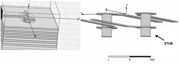
The 24-layer circuit board structure shown in Figure 1 is established in the HFSS software, the signal layer is the third layer, and the signal line is a strip differential line.
Schematic diagram of the simulation structure
1.2.2 Simulation parameter settings
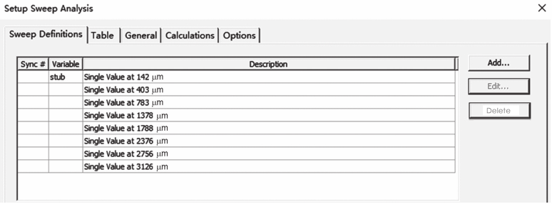
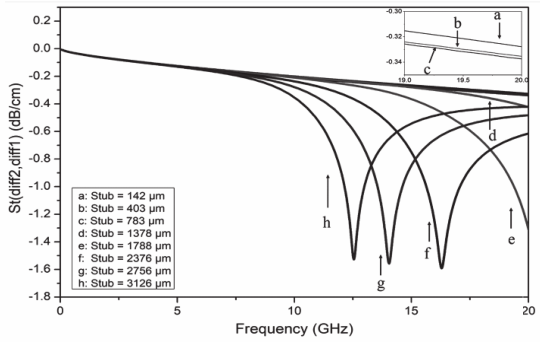
Set the sweep frequency range from 0 to 20 GHz, and set up 8 groups of stubs as shown in Figure 2, which are the signal layers L3 to L4, L6, L9, L12, L15, L18, L21, and L24. The corresponding lengths are 142, 403, 783, and 1378. , 1788, 2376, 2756, 3126 μm.
1.3 Test board production
1.3.1 Test board production
Due to the need to test the signal difference of different backdrilling depths, the stack structure adopts a 24-layer design, and the plate thickness is controlled at (3.30±0.33) mm. The specific stack structure is shown in the figure.
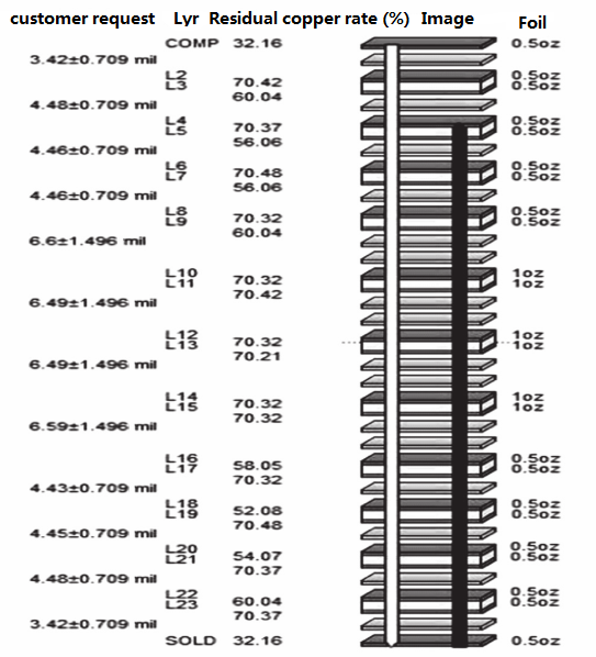
Stacking diagram
Signal layer: L3, reference layer: L2/L4. Signal hole diameter: 0.25 mm; 7 ground holes are through holes, diameter: 0.25 mm;
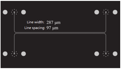
The transmission line is designed as a strip differential line as shown in Figure 4, with a differential impedance of 100 Ω. Line width: 97 μm, line spacing: 284 μm. Design 8 pairs of long and short differential lines, line length: (254/50.8) mm, drill through L4, L6, L9, L12, L15, L18, L21 respectively. The remaining group is not back-drilled and marked with the number (1) to (8).
1.3.2 Production process
Inner layer pattern transfer→AOI→pressing→drilling→electroplating→pattern electroplating→tin plating→back drilling→alkali etching→AOI solder mask→nickel-gold→forming
1.3.3 Preparation of samples
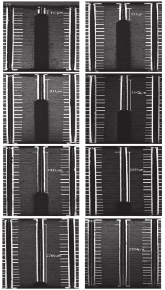
In order to accurately obtain the stub length, back-drilled cross-section slices need to be prepared for observation. Remove the sample from the test plate, polish it with 180#, 400#, 2400#, 4000# metallographic water sandpaper successively, and then treat it with polishing liquid. Then clean the polished samples, observe and measure the stub length of each group of samples under a metallographic microscope.
|2.Results and discussion
2.1 Simulation results and analysis
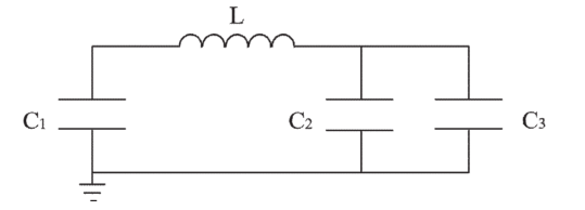
Figure 5 shows the insertion loss of the simulation model. As the length of the stub increases, the insertion loss also increases accordingly. When the stub is larger than 1378 μm, the signal loss increases significantly, and the resonance point appears within 20 GHz. When the via stub lengths are 237 μm, 2756 μm, and 3126 μm, resonance occurs at 12.5, 13.5, and 16.5 GHz, respectively. According to the via model, an equivalent circuit as shown in Figure 6 can be established, where L represents the via transmission line, C1 and C2 represent the equivalent capacitance structure formed between the pad and the reference ground, and C3 represents the stub. When the signal is transmitted through the hole, the stub acts as a miniature antenna. Since the smaller the antenna size, the higher the operating frequency (resonant frequency), so the stub becomes longer and the resonant frequency becomes smaller, which affects signal transmission.
2.2 Test Board Verification and Analysis
Figure 7 shows the stub lengths of 8 groups of samples observed and measured in a metallographic microscope. From Table 1, it can be seen that the actual length of the stub is different from the expected design value, which is due to the accuracy of the processing equipment and the thickness tolerance and other factors.
| Sample serial number | 1 | 2 | 3 | 4 | 5 | 6 | 7 | 8 |
| Design value (μm) | 142 | 403 | 783 | 1378 | 1788 | 2376 | 2756 | 3126 |
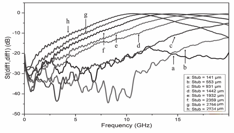
| Actual value (μm) | 141 | 553 | 931 | 1442 | 1932 | 2359 | 2766 | 2934 |
Table 1 Stub length comparison table
The figure below shows the comparison of the insertion loss of 8 groups of differential lines on the test board from 0 to 20 GHz. It can be seen that the shorter the stub, the smaller the insertion loss. The insertion loss of (0~5) GHz is relatively less affected by the stub length. When the signal frequency is 5 GHz, the maximum difference of insertion loss between each group of samples is 0.046 dB/cm. Starting from 5 GHz, the insertion loss of the four groups of samples with long stubs has begun to decrease significantly, and the four groups of samples with stubs of (1932, 2359, 2766, 2934) μm resonate at 16.4 GHz, 13.9 GHz, 11.8 GHz, and 10.8 GHz, respectively. . Samples with a stub smaller than 1442 μm have no resonance point in (0~20) Ghz. When stub = 1442 μm, the insertion loss has begun to drop significantly at high frequencies, indicating that the resonance point is very close to 20 GHz. The insertion loss of the three groups of samples with shorter stubs at 20 GHz differs by a maximum of 0.14 dB/cm.
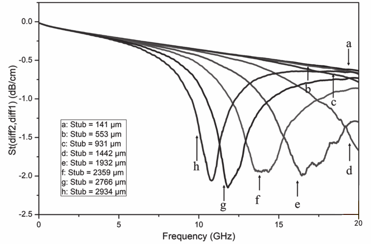
It can be seen that compared with the insertion loss curve of the actual test board, the general trend of insertion loss changes is consistent, and the loss increases with the length of the stub. However, because the simulation model is an ideal model, the surface of the line and the copper hole are smooth, so the signal loss is small, and the corresponding insertion loss value is correspondingly smaller, and the resonance points with longer stubs are also moved back. But the simulation results can still guide the design optimization of the PCB structure.
In printed circuit board design, the smaller the return loss value, the smaller the signal transmission loss. Figure 9 shows the return loss of the test board. It can be seen that the return loss generally shows an upward trend. The return loss of samples with Stubs of (1932, 2359, 2766, 2934) μm at frequencies of 16.4 GHz, 13.9 GHz, 11.8 GHz, and 10.8 GHz, respectively, has a turning point, which may be related to the resonance of the transmission signal. When the frequency increases to 20 GHz, the return loss value of the sample with a stub length of 141 μm is 19.49 dB, indicating that the attenuation of the signal power is small, which is beneficial to the transmission of high-frequency signals.
|3.Conclusion
The article simulates the signal of the 24-layer circuit board back-drilling structure and then makes a test board for verification. For the circuit board with low signal frequency (Frequency < 3 GHz), the stub length has relatively little influence on the signal integrity, and the back-drilling accuracy is required. It can also reduce and save costs. However, when the signal transmission frequency is high, the resonant frequency point corresponding to the longer stub is lower, which will significantly affect the signal integrity. Therefore, for high-frequency circuit boards, it is not only necessary to do back-drilling treatment, but also requires high back-drilling accuracy.
If you have any PCB demands, please feel free to contact us.
Email:[email protected]
Skype:[email protected]
Telephone number:+86 133 9241 2348
Whatsapp: +86 133 9241 2348