The countless small holes we see on PCBs are technically called vias, which are actually the only way to change layers of wiring. Figure 1 below shows the three typical types of vias on our PCB, namely through hole vias, blind vias, and buried vias.
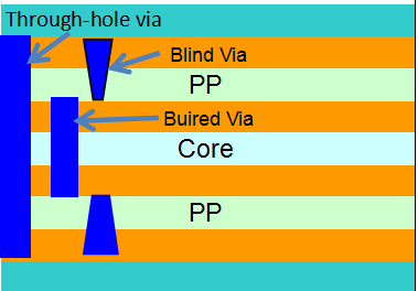
Most of the situations we usually encounter are pure through-hole PCBs. Boards that encounter blind holes may be caused by very high PCB layout density. Some high-pin-number devices are attached to the front and back, and then blind holes are drilled to solve the high-density problem. Of course, the cost will also increase compared to the cost of through holes. After there are blind holes, the PCB will generally be called HDI PCB (HDI means high density). Buried vias are rarely used. They may be like buried capacitors (capacitors hidden inside the PCB), which are very rare.
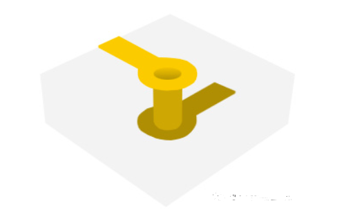
A through hole connects the traces on different layers together as shown in the picture below. The commonly used through holes we use are generally mechanical drilling (there are other mechanical holes, such as laser holes). First laminate all the layers of the PCB. After laminating into one PCB, drill through the PCB one by one like a nail to form through holes one by one. The inside of the through hole needs to be copper plated, and there is a relatively large circular metal disk called a pad at the signal connection. Of course, when a Via passes through all layers, if there is no connection on a certain layer, there will not be a large hole plate on this layer, but on the contrary, there will be an anti-pad. The anti-pad can be simply understood as a forbidden area that prevents vias from contacting a layer of metal copper foil. The anti-pad is actually very critical. Especially in high-speed and high-frequency PCB design, you will often hear engineers say “dig the anti-pad”.
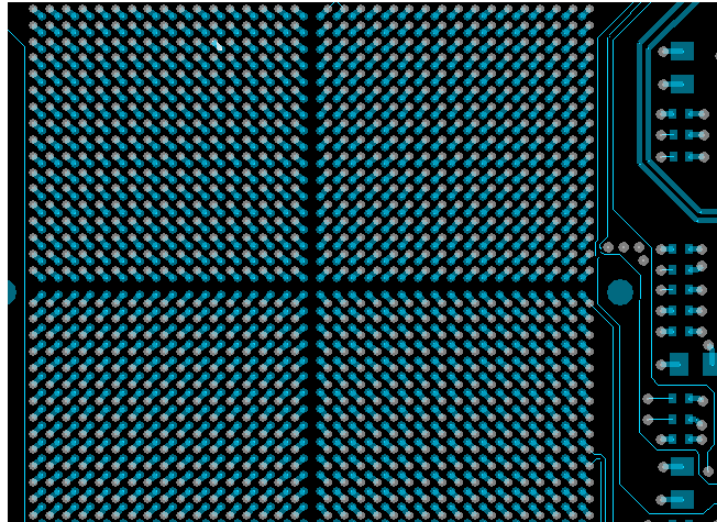
In PCB design, such as large BGA chips and multi-row connectors, a large area of FANOUT is required to guide the signal to the inner layer through nearby via holes. The picture below shows a BGA chip with thousands of pins. When performing FANOUT, it always feels beautiful. Based on the current size of our chip pins and the PCB thickness-to-aperture ratio (thickness-to-diameter ratio) processing requirements for vias, most of our commonly used vias have apertures of 8mil, 10mil, and 12mil.