The application of HDI is becoming more and more extensive in the electronics industry, especially under the current trend of miniaturization of electronic products. For the same product, choosing HDI designs with different structures will have a great impact on the cost.
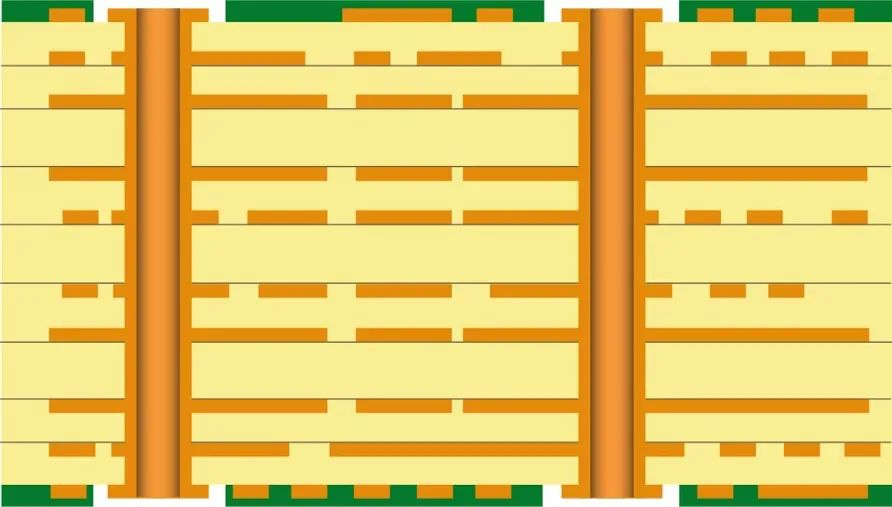
The above figure shows a 10L PCB built on a standard multi-layer process. There is no special process, just standard vias, traces and spacing within the process.
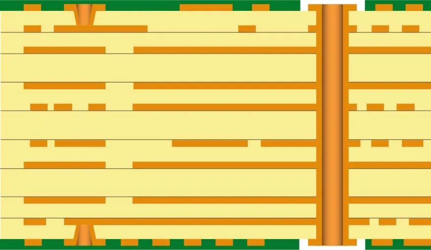
The picture above shows a 10L PCB with I-type HDI structure. Adding two layers of micro-vias means more laser drilling.Compared with the standard structure, the cost increases by 40%-70%.
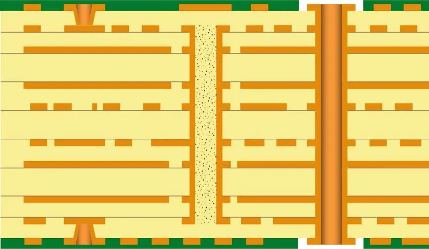
The picture above shows a 10L PCB with type II HDI structure. The increased buried hole structure means more drilling, electroplating and lamination steps.Compared with the standard structure, the cost increases by 80%-120%.
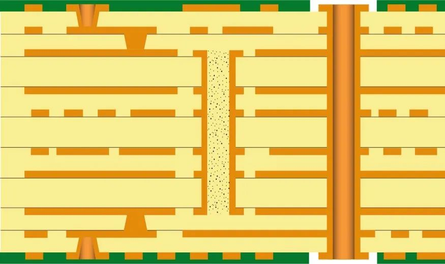
The picture above shows a 10L PCB with type III HDI structure. More buried via structures means more drilling (4), more plating (3) and more lamination steps (3).Compared with the standard structure, the cost has increased by 180%-200%+.
In your opinion, is the above-mentioned range of HDI cost fluctuations of different structures accurate?
Not really.
The cost here is fluctuating, without taking into account the changes in the number of PCB layers or dimensions… These are all key factors that will change after the introduction of HDI structure. Different product designs are different, and the more complex the design, the greater the impact on cost.
Any PCB need production please Contact us freely! RunTek PCBs Factory email:[email protected]