What is PCB copper cladding? Copper pouring is to use the idle space on the PCB as the reference plane, and then fill it with solid copper. These copper areas are also called copper pouring.
The significance of copper cladding is: reducing the impedance of the ground wire and improving the anti-interference ability; reducing the voltage drop and improving the power efficiency; connecting with the ground wire can also reduce the loop area, etc. There are generally two basic ways of copper cladding, that is, large area copper cladding (solid copper cladding) and grid copper cladding. Which is better for large area copper cladding or grid copper cladding? It’s hard to generalize, they each have their pros and cons.
1.Advantages of solid copper cladding: it has the dual functions of increasing current and shielding. Disadvantages: If it is wave soldered, the board may warp or even blister. Solution: Generally, several slots will be opened to relieve copper foil blistering.
2.Advantages of grid copper cladding: From the point of view of heat dissipation, the grid is good (it reduces the heating surface of copper) and plays a certain role in electromagnetic shielding. Disadvantages: The pure copper grid is mainly used for shielding, and the effect of increasing the current is reduced.
The pros and cons of copper cladding
Advantage:
Provides additional shielding protection and noise suppression for inner signal. Improve the heat dissipation capacity of the PCB. In the PCB production process, the amount of corrosive agents is saved.
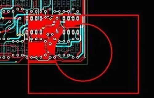
Avoid PCB warping and deformation caused by different stress generated during PCB reflow soldering due to unbalanced copper foil.
Disadvantages:
The copper-clad plane on the outer layer will definitely be fragmented by the components and signal lines on the surface. If there is a poorly grounded copper foil (especially the slender and long broken copper), it will become an antenna and generate EMI. question.
If the component pins are fully connected with copper, it will cause the heat to dissipate too quickly, making it difficult to desolder and rework. The copper-clad plane of the outer layer must be well grounded, and more vias need to be drilled to connect to the main ground plane. Too many vias will inevitably affect the wiring channel unless buried blind vias are used.
Precautions for copper cladding
When engineers are pouring copper, in order to achieve the expected effect of copper pouring, they need to pay attention to the following aspects:
1. If there are many grounds on the PCB, such as SGND, AGND, GND, etc., according to the different positions of the PCB surface, the most important “ground” is used as the reference to independently cover copper, digital ground and analog ground. There is not much to say about the copper coating separately. At the same time, before the copper coating, the corresponding power supply lines are first thickened: 5.0V, 3.3V, etc. In this way, multiple deformable structures of different shapes are formed.
2.For single-point connection of different grounds, the method is to connect through 0 ohm resistance or magnetic beads or inductance.
3. Copper cladding near the crystal oscillator. The crystal oscillator in the circuit is a high-frequency emission source. The method is to wrap copper around the crystal oscillator, and then ground the shell of the crystal oscillator separately.
4. The island (dead zone) problem, if you think it is too big, then it will not cost much to define a ground via and add it.
5. At the beginning of wiring, the ground wire should be treated equally, and the ground wire should be routed well when routing. You cannot rely on the addition of vias after copper coating to eliminate the ground pin for connection. This effect is very bad.
6. It is best not to have sharp corners on the board.
7. Do not cover the open area of wiring in the middle layer of the multi-layer board. Because it is very difficult for you to make this copper pour “good ground”.
8. Metals inside the equipment, such as metal radiators, metal reinforcement bars, etc., must be “well grounded”.
Summary: The copper on the PCB, if the grounding problem is dealt with properly, is “pros outweigh the cons”, it can reduce the return area of the signal line and reduce the external electromagnetic interference of the signal.
If you have any PCB demands, please feel free to contact us.
Email:[email protected]
Skype:[email protected]
Telephone number:+86 133 9241 2348
Whatsapp: +86 133 9241 2348