As a PCB design engineer, we all know that the impedance should be continuous. There is always a time when the impedance cannot be continuous in PCB design. What should I do at this time?
About Impedance
To clarify a few concepts first, we often see impedance, characteristic impedance, and instantaneous impedance. Strictly speaking, they are different, but invariably they are still the basic definition of impedance:
- The input impedance at the beginning of the transmission line is referred to as impedance;
- The real-time impedance encountered by the signal at any time is called the instantaneous impedance;
- If the transmission line has a constant instantaneous impedance, it is called the characteristic impedance of the transmission line.
Characteristic impedance describes the transient impedance that a signal experiences as it propagates along a transmission line, which is a major factor affecting signal integrity in transmission line circuits.
Unless otherwise specified, the characteristic impedance is generally referred to as the transmission line impedance. The factors that affect the characteristic impedance are: dielectric constant, dielectric thickness, line width, and copper foil thickness.
What is Impedance Continuous
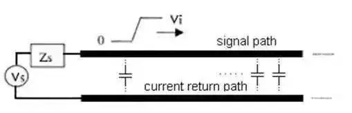
The impedance is continuous and similar: the water flows steadily in a uniform ditch, and suddenly the ditch turns and widens. Then the water will slosh around the bend, and water waves will propagate. This is the result of impedance mismatch.
Impedance discontinuity solution
1) Gradient line
Some RF device packages are small, the SMD pad width may be as small as 12mils, and the RF signal line width may be more than 50mils. Gradient lines are used, and line width sudden changes are prohibited. The gradient line is shown in the picture, and the line in the transition part should not be too long.

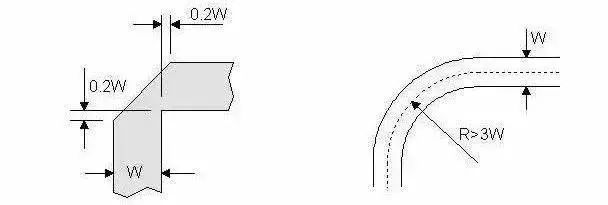
2) Corner
If the RF signal line runs at a right angle, the effective line width at the corner will increase, and the impedance will be discontinuous, causing signal reflection. To reduce discontinuities, there are two ways to deal with corners: chamfering and filleting. The radius of the arc angle should be large enough. Generally speaking, it should be ensured that: R>3W. As shown below.
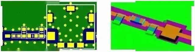
3) Large pad
When there is a large pad on the 50-ohm microstrip line, the large pad is equivalent to distributed capacitance, which destroys the continuity of the characteristic impedance of the microstrip line. Two methods can be taken at the same time to improve: firstly, thickening the microstrip line medium, and secondly, hollowing out the ground plane under the pad, both of which can reduce the distributed capacitance of the pad. As shown below.
4) Via
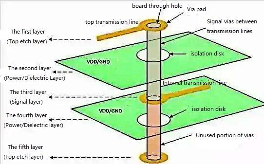
Vias are metal cylinders plated out of the through holes between the top and bottom layers of a circuit board. Signal vias connect transmission lines on different layers. Via stubs are unused parts of a via. Via pads are annular pads that connect vias to top or internal transmission lines. Isolation pads are annular voids within each power or ground plane to prevent shorts to the power and ground planes.
- Parasitic Parameters of Vias
After rigorous physical theory derivation and approximate analysis, the equivalent circuit model of a via can be a grounding capacitor connected in series at both ends of an inductor, as shown in the figure below.
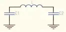
- Equivalent circuit model of vias
It can be seen from the equivalent circuit model that the via itself has parasitic capacitance to the ground. Assume that the diameter of the via anti-pad is D2, the diameter of the via pad is D1, the thickness of the PCB board is T, and the dielectric constant of the board substrate is ε, the parasitic capacitance of the via is approximated by:

The parasitic capacitance of the via can cause the signal rise time to be prolonged and the transmission speed to be slowed down, thereby deteriorating the signal quality.
Similarly, vias also have parasitic inductance. In high-speed digital PCBs, parasitic inductance is often more harmful than parasitic capacitance.
Its parasitic series inductance will weaken the contribution of the bypass capacitor, thereby reducing the filtering effect of the entire power system. Suppose L is the inductance of the via, h is the length of the via, and d is the diameter of the center hole. The approximate parasitic inductance size of a via is approximately:

Vias are one of the important factors that cause impedance discontinuity on the RF channel. If the signal frequency is greater than 1GHz, the influence of vias should be considered.
Common methods to reduce the discontinuity of via impedance include: using a diskless process, selecting a lead-out method, optimizing the diameter of the anti-pad, etc. Optimizing the anti-pad diameter is a common method to reduce impedance discontinuities.
Since the characteristics of the via hole are related to the structure size of the aperture, pad, anti-pad, stack structure, and lead-out method, it is recommended to use HFSS and Optimetrics for optimization simulation according to the specific situation in each design.
When a parametric model is employed, the modeling process is simple. During the review, the PCB designer is required to provide corresponding simulation documents.
Via diameter, pad diameter, depth, and anti-pad, all bring variations, resulting in impedance discontinuities, the severity of reflection and insertion loss.
5) Through hole coaxial connector
Similar to the via structure, through-hole coaxial connectors also have impedance discontinuities, so the solution is the same as vias. The common methods to reduce impedance discontinuity of through-hole coaxial connectors are also: using diskless technology, suitable wire exit method, and optimizing the diameter of anti-pad.
If you have any PCB demands, please feel free to contact us.
Email:[email protected]
Skype:[email protected]
Telephone number:+86 133 9241 2348
Whatsapp: +86 133 9241 2348