This first-order, second-order is to talk about the HDI manufacturing process of this PCB processing.
What is HDI?
HDI: short for high Density interconnection, high-density interconnection, non-mechanical drilling, micro-blind hole ring below 6mil, wiring width/line gap between inner and outer layers below 4mil, pad diameter not more than 0.35mm Laminate manufacturing method is called HDI board.
Blind via: short for Blind via, which realizes the connection between the inner layer and the outer layer
Buried hole: Abbreviation of Buried via, which realizes the connection and conduction between the inner layer and the inner layer
Blind holes are mostly small holes with a diameter of 0.05mm~0.15mm. The hole forming methods of buried blind holes include laser hole forming, plasma etching hole and photoinduced hole forming. Laser hole forming is usually used, and laser hole forming is divided into CO2 and YAG. Ultraviolet laser machine (UV).
HDI board sheet
- HDI board materials include RCC, LDPE, FR4
RCC: The abbreviation of Resin coated copper, resin coated copper foil. RCC is composed of copper foil and resin whose surface has been roughened, heat-resistant, anti-oxidation, etc., and its structure is shown in the figure below: (used when the thickness is >4mil)
The resin layer of RCC has the same processability as FR-4 adhesive sheet (Prepreg). In addition, the relevant performance requirements of the laminated multilayer board must be met, such as:
(1) High insulation reliability and micro-via reliability;
(2) High glass transition temperature (Tg);
(3) Low dielectric constant and low water absorption;
(4) High adhesion and strength to copper foil;
(5) The thickness of the insulating layer is uniform after curing
At the same time, because RCC is a new product without glass fiber, it is beneficial to the pitting treatment of laser and plasma, and is conducive to the lightweight and thinning of multilayer boards. In addition, resin-coated copper foil has thin copper foils such as 12pm and 18pm, which are easy to process.
What is a first-order, second-order PCB?
This first-order, second-order refers to the number of laser holes, how many times the PCB core board is pressed, and how many laser holes are punched! Just a few steps. As follows

- After pressing once, drill holes == “press the copper foil outside again ==” and then laser drill
This is first order , as shown in the figure below
- After pressing once, drill holes == “press the copper foil again on the outside == “laser again, drill == “press the copper foil on the outer layer again ==” laser drill again
This is second order. It mainly depends on how many times you have received laser treatment, that is, how many steps.
There are two kinds of stacked holes and bifurcated holes in the second order.
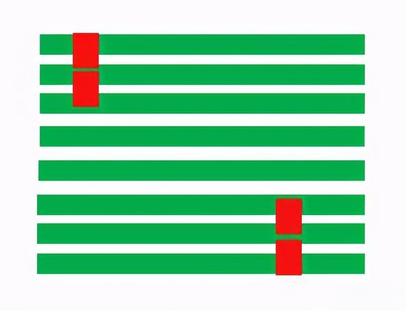
The picture below shows eight layers of second-order stacked holes. Layers 3-6 are pressed together first, and the outer layers 2 and 7 are laminated, and a laser hole is punched once. Laminate layers 1 and 8 on top and punch a laser hole again. It is to drill two laser holes. Because such holes are superimposed, the process difficulty will be higher and the cost will be higher.

The figure below shows the eight-layer second-order cross blind hole. This processing method is the same as the above eight-layer second-order stacked hole, and it also needs to drill two laser holes. But the laser holes are not stacked together, so the processing difficulty is much less.

The third-order and fourth-order PCBs are analogized in turn.