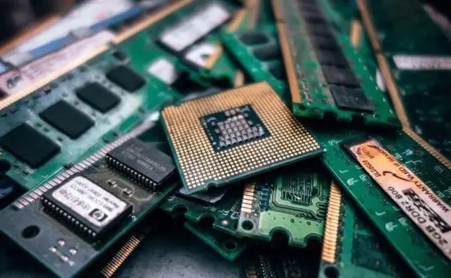
Gold Finger
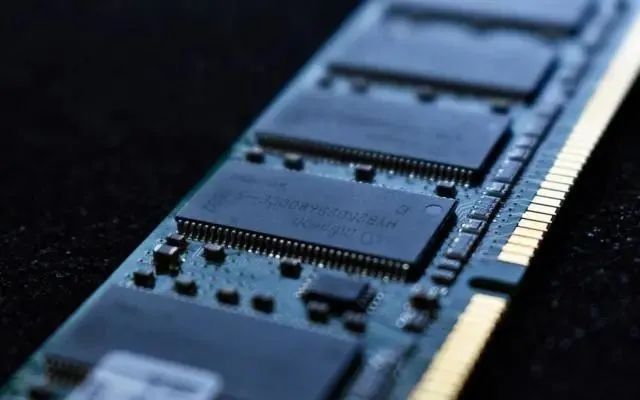
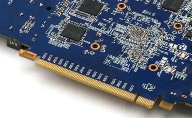
On computer memory sticks and graphics cards, we can see a row of golden conductive contacts, which are called “gold fingers”. The Gold Finger (or Edge Connector) in the PCB design and production industry uses the plug of the connector as the outlet for the external connection of the board to the network. Next, let’s take a look at the processing method and some details of the gold finger in the PCB.
Surface treatment of golden finger PCB
- Electroplated nickel gold: the thickness can reach 3-50u”, because of its excellent electrical conductivity, oxidation resistance and wear resistance, it is widely used in gold finger PCBs that need to be plugged frequently or PCB boards that need to be mechanically rubbed frequently The above, but because the cost of gold plating is extremely high, it is only used for local gold plating such as gold fingers.
- Immersion gold: the thickness is conventional 1u”, up to 3u”. Because of its excellent conductivity, flatness and solderability, it is widely used in high-precision PCB boards with key positions, binding IC, BGA and other designs. For gold finger PCBs that do not require high wear resistance, the whole board immersion gold process can also be selected. The cost of the immersion gold process is much lower than that of the electro-gold process. The color of the immersion gold process is golden yellow.
Detail processing of gold fingers in PCB
1) In order to increase the wear resistance of the gold finger, the gold finger usually needs to be electroplated with hard gold.
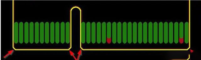
2) Gold fingers need to be chamfered, usually 45°, other angles such as 20°, 30°, etc. If there is no chamfer in the design, there is a problem; a 45° chamfer in the PCB looks like this:
3) The gold finger needs to be treated with a whole block of solder mask to open the window, and the PIN does not need to open the steel mesh;
4) Immersion tin and immersion silver pads need to be at a minimum distance of 14mil from the top of the finger; it is recommended that the pad should be more than 1mm away from the finger position during design, including via pads;
5) Do not spread copper on the surface of the gold finger;
6) All layers of the inner layer of the gold finger need to be cut copper, usually the width of the copper cut is 3mm larger; it can be used to cut copper for half fingers and for the whole finger.
Is Goldfinger’s “gold” gold?
First, let’s understand two concepts: soft gold and hard gold. Soft gold, generally softer gold. Hard gold is generally a compound of hard gold.
The main function of the gold finger is to connect, so it must have good electrical conductivity, wear resistance, oxidation resistance and corrosion resistance.
Because pure gold (gold) is relatively soft, gold fingers generally do not use gold, but only a layer of “hard gold (gold compound)” is electroplated on it, which can not only obtain good electrical conductivity of gold, but also make it resistant to Grinding performance, anti-oxidation performance.
So has PCB ever used “soft gold”? The answer is, of course, there is use, such as the contact surface of some mobile phone buttons, the aluminum wire on the COB (Chip On Board), etc. The use of soft gold is generally to precipitate nickel gold on the circuit board by electroplating, and its thickness control is more flexible.