Although HDI PCB fabrication can be expensive, there are several situations where blind vias, buried vias, and microvias offer a cost-effective solution.
High Density Interconnect (HDI) circuit board designs have a higher wiring and pad density than conventional PCBs, along with smaller trace widths and spaces. They require advanced PCB technologies such as blind vias, buried vias, and microvias. HDI PCBs are usually more costly than conventional PCBs due to the complex build-up process involved in fabrication.
Although HDI PCB fabrication can be expensive, there are several situations where blind vias, buried vias, and microvias can offer a cost-effective solution.Among China pcb manufacturers, who can produce HDI pcb boards, the price varies a lot once it includes blind vias, buried vias, and microvias.
(Even so, it is much more expensive for blind via board compared to standard boards, it is normally 200% or even up to 500% higher)Here are just a few scenarios where advanced PCB technologies may actually reduce the overall manufacturing cost.
Scenario 1: Reduce layer count by widening the BGA breakout channel with a blind via
If you’re using through-hole vias for a design and the trace escape for a ball grid array (BGA) isn’t going smoothly, consider widening the breakout channels on the bottom and inner layers with blind vias.Consider the illustration below. The board on the top had three rows of through-hole vias, letting only four traces out between the 1st and 3rd rows.
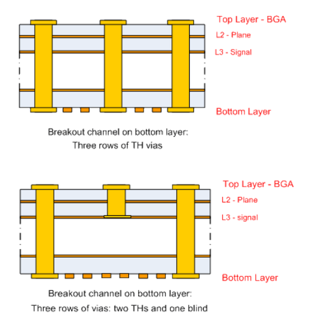
By comparison, in the case of the board on the bottom, the via in the middle has been replaced with a blind via. The same channel now permits six traces, which equates to a 50% increase. This technique may allow you to reduce the layer count of your PCB and — in turn — reduce the cost.
Scenario 2: Eliminate electrical layers by replacing through-hole vias with microvias
Microvias have the smallest pad size (as little as 0.008″), which helps maximize routing channel width. As in the previous scenario, replacing through-hole vias with microvias can ease BGA breakout and reduce the PCB layer count. When an inner signal layer is eliminated, its reference plane can sometimes be removed too, thus eliminating two layers.
The illustration below demonstrates one of the techniques that can be used to maximize breakout between microvias for a 1.0mm pitch BGA:If placing the microvias for maximum breakout, the gain will be 67%. If placing the microvias at the same grid as the through-hole vias, the breakout gain would be 33%. and if you send the updated gerber with new finished design with above recommendation to one of the China manufacturing , like ALLPCB or any other companies, they will caculate it based on new file and price will most likely lower.
Scenario 3: Use blind and buried vias to reduce the PCB aspect ratio
Often, a PCB will have BGA components with several different pitches. For example, there may be a 1.27mm pitch BGA and an 0.8mm pitch BGA on a 4.0mm (160mil)-thick PCB. The minimum via hole is not only determined by drill size, but also the aspect ratio, which is the thickness of the PCB divided by the diameter size of the drilled hole:There is usually an additional manufacturing cost for aspect ratios higher than 10 or 12. (Note that the finished hole size is ~2mil less than the drilled hole size; this due to the width of the barrel plating.)
If through-hole vias are still required, even after blind/micro/buried vias are used, it may be a challenge keep the aspect ratio low. An aspect ratio of 12 on a 4mm board would mean that the minimum finished through-hole via size is 0.3mm (12mil), which corresponds to a drill hole size of 0.36mm (14mil) and pad size of 0.56mm (22mil). This would be fine for the 1.27mm pitch BGA, but would raise concerns for the 0.8mm pitch BGA, since the via pad-to-BGA pad clearance would only be 0.09 (3.4mil) with 0.4mm (15.7mil) BGA pads.
To meet the aspect ratio requirements, the PCB thickness would have to be reduced as follows: -3.6mm (140mil) for 10mil through-hole vias (drill size of 12mil) with 0.5mm (20mil) pads for the 0.8mm pitch BGA-3.0mm (120mil) for 8mil through-hole vias (drill size of 10mil) with 0.45mm (18mil) pad for the 0.8mm pitch BGA
If you reduce the layer count by replacing through-hole vias with blind vias and microvias, you can achieve a smaller aspect ratio for your PCB, and avoid any cost penalties due to using blind/microvias.
These are just three scenarios where advanced PCB technology may be cost-effective for your design. Look for many more unique situations soon, as PCB fabrication equipment and materials continue to progress.
If you have any PCB demands, please feel free to contact us.
Email:[email protected]
Skype:[email protected]
Telephone number:+86 133 9241 2348
Whatsapp: +86 133 9241 2348