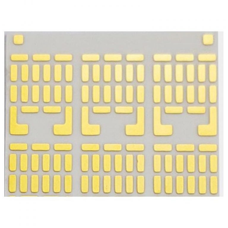
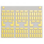
What is ceramic PCB?
Ceramic PCB is a kind of heat conducting ceramic powder and organic binder, and the heat conduction organic ceramic PCB is prepared at a thermal conductivity of 9-20W/m. In other words, ceramic PCB is a printed circuit board with ceramic base material, which is highly thermally conductive materials such as alumina, aluminum nitride, as well as beryllium oxide, which can make a quick effect on transferring heat away from hot spots and dissipating it over the whole surface. What’s more, ceramic PCB is fabricated with LAM technology, which is a laser rapid activation metallization technology. So ceramic PCB is highly versatile that can take place of the entire traditional printed circuit board with a less complicated construction with enhanced performance.
With the development of chip components and surface mount technology (SMT) in electronics industry, traditional printed circuit boards with organic laminates as based material are developing towards high density, high precision, and high reliability. Needless to say, ceramic PCB, as a relatively new type of printed circuit board, which has been widely used in electronics industry for years, and it is a more viable option for PCB designers, considered as an effective solution for miniaturization accomplishment of modern electronics products and electronic assembly technology. You will find that ceramic PCB has an advantage over traditional printed circuit board, what’s more, ceramic PCB is more versatile, less complex and offer superior performance because of its high thermal conductivity and minimal expansion coefficient (CTE).
Types of ceramic PCBs
There are three main types of ceramic PCB in the electronic market based on the manufacturing method.
- High temperature ceramic PCB
- Low temperature ceramic PCB
- Thick film ceramic PCB
High temperature
As you know, high temperature may be the most popular types pf ceramic. In general, The ceramic PCB designed for high temperatures is often regarded as high temperature co-fired ceramic (HTCC) circuit, which is made up of raw ceramics with solvent, mixing adhesive, plasticizer, lubricant as well as aluminum oxide.
First of all, it fabricates with the raw ceramic material, secondly coat the material, and then carry out the circuit tracing on tungsten or molybdenum metals. Finally, if the circuit tracing is achieved, it can bake the boards between 1600 and 1700 degrees Celsius for up to 48 hours after lamination. All HTCC baking is done in a gaseous environment, such as in hydrogen gas.
Low temperature
Unlike HTCC, low temperature co-fired ceramic PCB is made up of combining crystal glass with an adhesive substrate on sheet metal with gold paste. And then cut and laminate the circuit board before placed in a gaseous oven at roughly 900 degrees Celsius.
What’s more, low temperature co-fired ceramic PCB profits by less warpage and evolutionary shrink tolerance. In other words, comparing to HTCC and other types of ceramic PCB, ceramic PCB has s better mechanical intensity and thermal conductivity. So as using the heat dissipation products such as LED lights, there is a advantage for the thermal benefit of LTCC.
Thick film ceramic
Thick film ceramic PCB, the thickness of its conductor layer may exceed 10 microns, but not more than 13 microns. In general, the conductor layer is printing the silver or gold palladium on the surface of ceramic PCB. That is to say, thick film ceramic PCB includes gold and dielectric pastes, which is done on a ceramic base material, and the pastes and backed at a temperature of 1000 degrees Celsius or below after working. So the thick film ceramic PCB is widely used for most PCB manufacturers because of the high cost of gold conductor paste.
The main advantage of thick film ceramic PCB over traditional PCB is that thick film ceramic can protect copper from oxidizing. So a ceramic PCB manufacturer can put interchangeable conductors, semi-conductors, conductors, electric capacitors, or resistors on the ceramic board. After achieving the process of printing and high-temperature sintering, all the components on the board can be laser-trimmed to their desired values.
There is a confusion about how many layers in a ceramic PCB, but it is decided by the types of ceramic PCB. The minimum number of layers used in ceramic PCB is two layers, however, there may be some more layers according to the product’s properties.
How to manufacture ceramic PCB?
First of all, It can use the silver or gold conductive pastes for placing trace connections in each layer in ceramic PCB fabrication process. In general, the metal elements or substrate are placed in each layer with a layer by layer screen printing process. In addition, it also can mechanically punch the vias in an unburned layer, or drill the microvias with a laser.
Secondly after printing and stacking the ceramic layers, it will bake the whole stack in an oven. In general, what the firing temperature needs for baking the ceramic PCB is below 1000 °C, which matches the sintering temperature of gold or silver pastes material. So the low temperature bake process is what allows the gold or silver in ceramic PCB.
However hot pressing/baking and sintering process for multilayer PCB makes it easy to integrate passive components immediately into the internal layers of a ceramic PCB. It is impossible in a board fabricated with FR-4 material, so the PCB designer can increase component and connection density on internal layers.
The advantages of ceramic PCB
Heat dissipation is the key benefit that ceramic has over more conventional materials such as FR-4 and metal clad PCB. Because the components are placed directly on the boards, and there is no isolation layer, the flow of heat through the boards is far more efficient. In addition, ceramic material can suffer from high operating temperatures (up to 350°C), what’s more, it has a quite low coefficient of thermal expansion (CTE), allowing for additional compatibility options for PCB design.
Compared with traditional PCBs whose substrate materials are epoxy glass fiber, polyimide, polystyrene and phenolic resin, ceramic PCBs feature the following properties:
- Excellent thermal conductivity
- Resist chemical erosion
- Compatible mechanical intensity
- Make it easy to implement high-density tracing
- CTA component compatibility
So it can be seen that the reasons why the ceramic PCB is so popular are as follows:
High thermal expansion
One reason why ceramic PCB is widely used in electronic industry is that because it has high thermal coefficient expansion. The ceramic base thermal conductivity arises being quite close to silicon, while under most used connection metals at the same time. Needless to say, it can play the part of great isolators for a long time. So there is optimum property for the high thermal conductivity of ceramic PCB even under elevated temperatures so that it can be used in many devices.
Stability
There is a stable dielectric property because of the use of ceramic, the balance can change into a limited radio frequency loss so that increasing the applicability of electronic device. What’s more, despite the outward toughness, ceramic has natural resistance for most chemical used because of the ceramic base PCB. Therefore, the resistance to chemical will change to resistance to daily moisture, solvents as well as consumables.
Versatility
It is no wonder that incorporation of metal core PCB can achieve a lot of applications with a high melting point. The noble metal paste can be highly unfailing conductors because of sintering technology. So there is no doubt that the use of ceramic PCB makes a effect on being high processing temperatures while there are different devices for different operating temperatures. What is interesting is the it also allows for good thermal conductivity and distribution of heat to the different position of a device.
Durability
As you know, there is a durability in the ceramic PCB fabrication process. Because of the essential properties of ceramics, specially the toughness, which can make sure that preventing your board from daily wear and tear. Because the ceramic PCB has a quite slow aging property with the consistency of based PCB, it can be changed without worry of replacement soon. What’s more, it has a high thermal resistance as it can change to a slowed decomposition process so that extends useful life length.
Adaptability
At last, one of the prominent advantages of ceramic PCB is that using the metal core in the engineering process. It can change to be the rigid carriers so that provides mechanical stiffness, making it easy to use between fluids and solids as the roughness and wear resistance are great, so it can be used in various industrial position.
What are the types of ceramic substrates?
A. According to the material
1). Al2O3
So far, the alumina substrate is the most commonly used substrate material in the electronics industry, because of its mechanical, thermal, and electrical properties compared to most other oxide ceramics, it has high strength and chemical stability, and is rich in raw materials. It is suitable for various technical manufacturing and different shapes.
2). BeO
It has a higher thermal conductivity than metal aluminum and is used in applications requiring high thermal conductivity, but the temperature drops rapidly after 300 ℃. The most important thing is that its toxicity limits its development.
3). AlN
There are two very important properties of AlN worth noting: one is high thermal conductivity, and the other is the expansion coefficient matching Si. The disadvantage is that even if there is a very thin oxide layer on the surface, it will affect the thermal conductivity. Only by strictly controlling the materials and processes can we produce an AlN substrate with good consistency. At present, compared to the AI2O3, the price of AlN is relatively high, which is also a small bottleneck restricting its development. However, as the economy improves and technology upgrades, this bottleneck will eventually disappear.
Based on the above reasons, it can be known that alumina ceramics are still in a dominant position in the fields of microelectronics, power electronics, hybrid microelectronics, and power modules due to their superior comprehensive performance, and are widely used.
B.According to the manufacturing process
1).HTCC (High-Temperature Co-fired Ceramic)
HTCC is also called high temperature co-fired multilayer ceramic. The manufacturing process is very similar to LTCC. The main difference is that HTCC’s ceramic powder is not added to glass materials. Therefore, HTCC must be dried and hardened at a high temperature of 1300 ~ 1600 ℃. Due to its high co-firing temperature, the choice of metal conductor materials is limited. Due to its high co-firing temperature, the choice of metal conductor materials is limited. The main materials are tungsten, molybdenum, manganese, etc., which have high melting points but poor conductivity, and are finally laminated and sintered to shape.
2).LTCC (Low-Temperature Co-fired Ceramic)
LTCC is also called low temperature co-fired multilayer ceramic substrate. This technology must first mix inorganic alumina powder with about 30% ~ 50% glass material with an organic binder to make it evenly mixed into a mud-like slurry. Use a scraper to scrape the slurry into a sheet, and then form a thin piece of the green embryo through a drying process, and then drill through holes according to the design of each layer as the signal transmission of each layer. The internal circuit of LTCC uses screen-printing technology to fill holes and print circuits on the green embryo respectively. The internal and external electrodes can use silver, copper, gold and other metals respectively. It can be completed by sintering it in a sintering furnace at 850 ~ 900 ℃.
3) DBC (Direct Bonded Copper)
Direct Bonded Copper technology uses copper’s oxygen-containing eutectic solution to directly deposit copper on the ceramic. The basic principle is to introduce an appropriate amount of oxygen between copper and ceramic before or during the deposition process. In the range of 1065 ℃ ~ 1083℃, copper and oxygen form a Cu-O eutectic liquid. The DBC technology uses this eutectic liquid to chemically react with the ceramic substrate to generate CuAlO2 or CuAl2O4. Also, it infiltrates the copper foil to achieve the combination of the ceramic substrate and the copper plate.
4).DPC (Direct Plate Copper)
DPC is also known as direct copper-plated substrate. Take the DPC substrate technology as the example: First, the ceramic substrate is pre-processed and cleaned, and it is sputtered and bonded to the copper metal composite layer on the ceramic substrate using the professional film manufacturing technology-vacuum coating method, and then the photoresist with yellow light lithography is re-exposed, developed, etched, and the film removal process is completed Line making Finally, the thickness of the circuit is increased by electroplating / electroless plating deposition. After the photoresist is removed, the metallization circuit is completed.
5). LAM (Laser Activation Metallization)
Using a high-energy laser beam to ionize ceramic and metal, let them grow together to make them firmly together.
Characteristics of LAM products:
- Higher thermal conductivity
- More matched thermal expansion coefficient
- The metal film with lower resistance
- The solderability of the substrate is good, and the use temperature is high
- Good insulation
- The thickness of the conductive layer can be customized within 1μm ~ 1mm
- Low frequency loss
- High-density assembly is possible
- Free of organic ingredients
- The copper layer does not contain an oxide layer
- Three-dimensional substrate & Three-dimensional wiring
Application of Ceramic PCB
- high-accuracy clock oscillator, voltage controlled oscillator (VCXO), temperature compensated crystal oscillators (TCXOs), oven controlled crystal oscillators (OCXOs);
- Semiconductor cooler;
- electric power electronic control module;
- high insulation & high pressure device;
- high temperature (up to 800C)
- high power LED
- High Power semiconductor modules
- solid state relay (SSR)
- DC-DC module power sources
- electric power transmitter modules
- Solar-panel arrays
Any Ceramic PCB projects need production please contact us freely! mail address: [email protected] or [email protected]