
Double sided smt pcb assembly quality control:
The production line is equipped with high-end equipment, high-precision and high-yield processing. * Carry out quality inspection and control in each processing link to prevent defective products from flowing into the next link. * Set up multiple quality personnel to conduct random inspections throughout the process.
(1) Glued cardboard: test whether the SMT placement position is correct, greatly reduce the SMT trial production time and the waste of components, and effectively ensure the quality of SMT
(2) Intelligent first piece detector: detects wrong materials, missing parts, polarity, orientation, silk screen, etc., mainly used in the first piece detection; compared with manual detection, the accuracy is higher and the speed is increased by 50%+
(3) SPI-Automatic 3D Solder Paste Thickness Gauge: Detects all kinds of solder paste printing quality problems such as missing printing, less tin, more tin, continuous tin, offset, poor shape, board surface pollution, etc.
(4) AOI: Detect various problems after placement: short circuit, material leakage, polarity, displacement, wrong parts
(5) Xray: Open circuit and short circuit detection of BGA, QFN and other devices
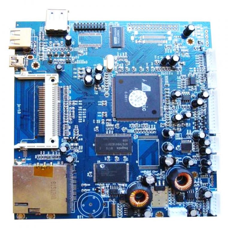
Double sided smt pcb assembly process
- Double-sided SMT mounting
In order to ensure the aesthetics and functionality of the PCB, some PCB design engineers will use double-sided mounting. Among them, IC components are arranged on the A side, and chip components are mounted on the B side. Make full use of the PCB board space to minimize the PCB board area.
- Double-sided mixed
There are two ways of double-sided mixing:
(1) The first method of PCBA assembly is heated three times, with low efficiency, and the use of red glue process wave soldering has a low pass rate and is not recommended.
(2) The second method is suitable for the situation where there are many double-sided SMD components and few THT components, and manual welding is recommended. If there are many THT components, wave soldering is recommended.
How to get a quote for Circuit Board Assembly (PCBA) Services?
1. PCBs Online Quote: You can get a PC board price instantly after a few option selections. All PCBs will be electrically tested. Click PCB Quote Online to get a quote now.
2. Labour Assembly online Quote: This is also an instant quote. You can get the labour assembly cost in seconds. Click PCB Assembly Quote to get a quote now.
3. BOM Pricing: Send your BOM (Bill of Materials) to email: [email protected] , we will email you the BOM price in 24 hours. BOM must include the quantities, reference designators, and manufacturer name and manufacturer part number.
4. If you already have your quote, then you are ready to place your order at your convenience!
See our comprehensive PCB Assembly Checklist for an overview of both the quotation and production processes.
Our Circuit Card Assembly Capabilities:
| Supported Capabilities | |
| Types of Assembly | THD (Thru-Hole Device) SMT (Surface-Mount Technology) SMT & THD mixed 2 sided SMT and THD assembly |
| Order quantity | 1 to 10,000 boards |
| Components | Passives parts, smallest size 0201 Fine pitch to 8 Mils BGA, uBGA, QFN,POP and Leadless chips Connectors and terminals |
| Component Package | Reels Cut tape Tube and tray Loose parts and bulk |
| Board dimensions | Smallest size: 0.2″ x 0.2″ Largest size: 15″ x 20″ |
| Board shape | Rectangular Round Slots and Cut outs Complex and Irregular |
| Board type | Rigid FR-4 Rigid-Flex boards |
| Assembly process | Leaded process Lead-Free (RoHS) |
| Design file format | Gerber RS-274X BOM (Bill of Materials) (.xls, .csv, . xlsx) Centroid (Pick-N-Place/XY file) |
| Sales and support | Emails Phone calls Web online quotation for PCB and assembly |
| Electrical testing | X-ray Inspection AOI (Automated Optical Inspection) Functional testing |
| Oven profile | Standard Custom |
| Turnaround time | 1-5 days for only PCB assembly 10-16 days for turnkey PCB assembly |
Testing Procedures
Various testing method will be applied to the assembled boards before the final shipment:
- Visual inspection: general quality check.
- FAI: full quality check applied to the first PCB to pass through all stages of production.
- X-ray Inspection: checks for BGAs, QFN and bare circuit boards.
- AOI Testing: checks for solder paste, 0201 components, missing components and polarity.
- 3D AOI Testing: checks for missing and misplaced SMT components in three dimensions.
- 3D SPI Testing: measures the precise volume of solder paste for SMT assembly.
- ICT (In-Circuit Test).
Functional test (Following your test procedures).
ISO Certification
RunTek PCB’s production facilities are ISO9001 certified to ensure we go beyond your expectations.