
What is PCB design?
Printed circuit board (PCB) design brings your electronic circuits to life in the physical form. Using layout software, the PCB design process combines component placement and routing to define electrical connectivity on a manufactured circuit board.
How to Design PCB?
How to design PCB boards is not easy to figure out, but the right pcb design software can go a long way. Other engineers have taken the time to learn the art of PCB design, and you can benefit from their experience. If you’re new to PCB design and you’re still learning about designing a custom circuit board in Altium Designer®, we’ve compiled the 10 important steps you can use to create modern PCB layouts for nearly any application.
There is a lot that goes into any engineered design, from a basic printed circuit to a complex non rigid PCB. Any new electronic device will start as a block diagram and/or a set of electronics schematics. Once you have your schematics finished and validated, you can follow the steps below to create modern PCB layouts in Altium Designer. Here’s the full list of PCB layout and design steps:
1. Create the Schematic
2.Create a Blank PCB Layout
3.Schematic Capture: Linking to Your PCB
4.Designing Your PCB Stackup
5.Defining Design Rules and DFM Requirements
6.Place Components
7.Insert Drill Holes
8.Route Traces
9.Add Labels and Identifiers
10.Generate Design Files
How to Design a Circuit Board in 10 Steps
When designing a circuit board it may sometimes seem as though arriving at the final design is going to be a long and arduous journey. Whether it’s the basics of micromanaging your copper and solder, or trying to ensure that your circuit board ends up printed after all, or going into more specific design problems such as through-hole technology or layout design with vias, pads, and any number of signal integrity issues, you’ll want to make sure you have the right design software.
If you’ve been doing this for decades, you don’t need me to tell you how valuable knowing your design software is to getting your printed boards designed right. Laying out traces for routing and copper placement, or managing the layer needed for solder can become difficult without an accurate and reliable integration from schematic capture to layout.
Though a deep program, Altium Designer’s user-experience is highly rewarding for new and experienced PCB designer experiences alike. It offers a design environment built from the ground up for a streamlined custom circuit board design process within a single, unified printed circuit board layout environment.
Step 1: Create the Schematic
Whether you are generating your design from a template or creating your printed circuit board from scratch, it is probably best to begin with the schematic. Your schematic is similar to the blueprints for your new device, and it is important to understand what is shown in your schematics. First, your schematics show you the following:
A.Which components are used in your design
B.How components are connected together
C.The relationships between groups of components in different schematics
The last point above is quite important, as complex designs may use hierarchical schematics. You can enforce significant organization in your new board if you take a hierarchical approach to your design and place different circuit blocks in different schematics. You can learn more about the value of well-designed schematics from Carl Schattke on the OnTrack Podcast.
Not only is circuit interconnectivity easier to define and edit, but converting a schematic to a board layout is much easier than designing directly on the board. For components, Altium Designer has an extensive database of parts libraries. Additionally, you can utilize the Altium Vault, which provides access to thousands of component libraries and adds flexibility to your project management and product development. However, you can also design your own schematic symbols and create footprints. Or, if you would like to have a part created for you, try Altium’s EE Concierge service.
Step 2: Create a Blank PCB Layout
After you’ve created your schematic, you’ll need to use the schematic capture tool in Altium Designer to start creating your PCB layout. First, create a blank printed circuit board document which will generate a PcbDoc file. This is done from the main menu in Altium Designer, as shown below.
If the printed circuit board shape, dimensions, and layer stackup for your board have already been determined, you can set them now. If you don’t want to do these tasks now, don’t fret, your board shape, size, and layer stackup (see Step 4 below) can be changed later. Schematic information is made available for the PcbDoc by compiling the SchDoc. The compilation process includes verifying the design and the generation of your several project documents that allow you to inspect and correct the design prior to transfer to the PcbDoc, such as those shown below. It is highly recommended that you review and update the Project Options at this point, which are used to create the PcbDoc information.
Step 3: Schematic Capture: Linking to Your PCB
All the tools in Altium Designer work in a united design environment, where the schematic, printed circuit board layout, and BOM are interlinked and can be accessed simultaneously. Other programs force you to manually compile your schematic data, but Altium Designer does this for you automatically while you create your design. To transfer SchDoc information to the newly created PcbDoc, click on Design » Update PCB {Filename of your new PCB}.PcbDoc. An Engineering Change Order (ECO) dialog will open listing all components and nets from the schematic, similar to the one below.
Verify the changes (addition of the SchDoc information to the project without error) by clicking on the Validate Changes tab. If the status for all items is green, then click on the Execute Changes tab. To complete the process, close the dialog.
Step 4: Designing Your PCB Stackup
When you transfer your schematic information to the PcbDoc the component footprints are shown in addition the board outline specified. Prior to placing components you should define the PCB layout (i.e. shape, layer stackup) using the Layer Stackup Manager, shown below.
If you’re new to the printed circuit design world, most modern PCB design concepts will start with a 4-layer board on FR4, although you can define any number of layers you like in Altium Designer. You can also take advantage of the Materials Stackup Library; this lets you choose from a range of different laminates and unique materials for your printed circuit board.
If you’re working on a high speed/high frequency design, you can use the built-in impedance profiler to ensure impedance control in your board. The impedance profile tool uses an integrated electromagnetic field solver from Simberian to tailor the geometry of your traces to meet a target impedance value.
Step 5: Defining Design Rules and DFM Requirements
The number of PCB design rule categories is extensive and you may not need to use all of these available rules for every design. You can select/deselect individual rules by right clicking on the rule in question from the list in the PCB Rules and Constraints Editor, below.
The rules that you do use, especially for manufacturing, should be inline with the specifications and tolerances for your PCB manufacturer’s equipment. Advanced designs, such as impedance controlled designs and a number of high speed/high frequency designs, may require very specific design rules that need to be followed in order to ensure your product works properly. Always check your component datasheets for these design rules. If necessary, you can create new design rules by following the steps of Altium Designer’s Design Rule Wizard.
Altium Designer will treat your custom design rules just like the built-in design rules. As you place components, vias, drill holes, and traces, the unified design engine in Altium Designer will automatically check the layout against these rules and will flag you visually if there is a violation.
Step 6: Place Components
Altium Designer provides a great deal of flexibility and allows you to quickly place components on your circuit board. You can have your components automatically arranged or you can place them manually. You can also use these options together, which allows you to take advantage of the speed of auto-placement and ensure your board is laid out according to good component placement guidelines. An added advanced feature of this latest version of Altium Designer is the ability to arrange components as groups. You can define these groupd in the PCB layout, or you can define groups on the schematic using Cross Select Mode, which is accessible from the Tools menu.
Step 7: Insert Drill Holes
Before routing your traces, it is a good idea to place your drill holes (mounting and vias). If your design is complicated you may need to modify at least some of the via locations during trace routing. This can be done easily from the via Properties dialog, shown below.
Your preferences here should be guided by the design for manufacturing (DFM) specifications of your PCB manufacturer. If you already defined your PCB DFM requirements as design rules (see Step 5), Altium Designer will automatically check these rules as you place vias, drill holes, pads, and traces in your layout.
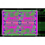
Step 8: Route Traces
Once you’ve placed your components and any other mechanical elements, you’re ready to route your traces. Be sure to utilize good routing guidelines and take advantage of Altium Designer tools to simplify the process, such as highlighting nets and color coding via routing, as shown below.
Altium Designer includes a number of important tools to help make your routing experience easier and more productive. You’ll have access to a powerful autorouter and auto-interactive routing tools. These tools will operate on multiple nets simultaneously, making it easy to route a large number of traces in tandem.
Step 9: Add Labels and Identifiers
With the circuit board layout verified you are ready to add labels, identifiers, markings, logo or any other imagery to your board. It is a good idea to utilize reference identifiers for components, as this will assist in PCB assembly. Also, include polarity indicators, pin 1 indicators and any other labels that are helpful in identifying components and their orientation. For logos and images, it is best to consult with your PCB manufacturer to ensure that you are using readable fonts.
Step 10: Generate Design Files
Before you create your manufacturer deliverables, it’s always a good idea to verify your circuit board layout by running a design rule check (DRC). Altium Designer will do this automatically as you layout your components and route your design, but it never hurts to run another DRC manually. If your board checks out, then you’re ready to release your manufacturer deliverables.
Once your board has passed the final DRC, you need to generate the design files for your manufacturer. The design files should include all the information and data necessary to build your board; including any notes or special requirements to ensure that your manufacturer is clear on what you require. For most manufacturers, you will be able to use a set of Gerber files as shown below; however, some manufacturers prefer other CAD file formats.
By following the above steps, the process of creating a comprehensive design is as easy as counting to ten. Using a systematic approach such as this ensures that all aspects of your design are accounted for inherently during the process, with minimal need to retrace your steps.
Altium Designer is an advanced PCB design and development package that provides you with many tools to simplify otherwise challenging design tasks. But, the functionality and capabilities discussed here only scratch the surface of what is available to you. To explore these and other options, test the program yourself with a free trial. For more information on designing a circuit board using Altium Designer, talk with an Altium Designer PCB design expert. You can also continue your learning journey by listening in to the Altium Podcast.