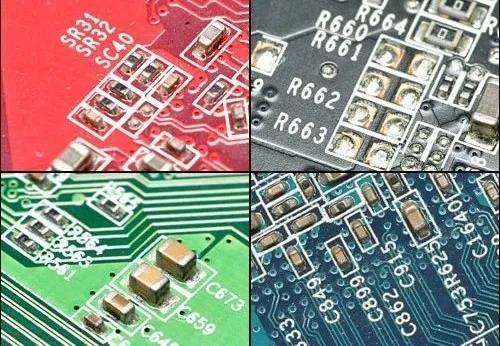
We will find that the PCB colors used by various board products in the market are dazzling. Common PCB colors are black, green, blue, yellow, purple, red, and brown. Some manufacturers have ingeniously developed PCBs of different colors such as white and pink.
In the traditional impression, black PCB seems to be positioned at the high end, while red, yellow, etc. are dedicated to the low end. Isn’t that true?
PCB copper layer that is not coated with solder mask is easily oxidized when exposed to the air.
We know that both sides of the PCB are copper layers. In the production of PCB, the copper layer will get a smooth and unprotected surface regardless of whether it is made by additive or subtractive methods.
Although the chemical properties of copper are not as active as aluminum, iron, magnesium, etc., in the presence of water, pure copper is easily oxidized by contact with oxygen; because oxygen and water vapor exist in the air, the surface of pure copper is exposed to air. Oxidation reaction will occur soon.
Since the thickness of the copper layer in the PCB is very thin, the oxidized copper will become a poor conductor of electricity, which will greatly damage the electrical performance of the entire PCB.
In order to prevent copper oxidation, to separate the soldered and non-soldered parts of the PCB during soldering, and to protect the surface of the PCB, engineers invented a special coating. This kind of paint can be easily applied to the surface of the PCB to form a protective layer with a certain thickness and block the contact between copper and air. This layer of coating is called a solder mask, and the material used is solder mask.
Since it is called lacquer, it must have different colors. Yes, the original solder mask can be made colorless and transparent, but PCBs often need to be printed with small text on the board for the convenience of maintenance and manufacturing.
The transparent solder mask can only reveal the PCB background color, so the appearance is not good enough whether it is manufacturing, repairing or selling. Therefore, engineers added a variety of colors to the solder mask to form a black, red, or blue PCB.
The black PCB is difficult to see the traces, which brings difficulties to maintenance
From this point of view, the color of the PCB has nothing to do with the quality of the PCB. The difference between black PCB and blue PCB, yellow PCB and other color PCBs lies in the color of the solder mask.
If the PCB design and manufacturing process are exactly the same, the color will not have any effect on performance, nor will it have any effect on heat dissipation.
Regarding the black PCB, since the traces on the surface are almost completely covered, it causes great difficulties in the later maintenance, so it is a color that is not convenient to manufacture and use.
Therefore, in recent years, people have gradually reformed, abandoning the use of black solder mask, and instead use dark green, dark brown, dark blue and other solder masks for the purpose of facilitating manufacturing and maintenance.
Having said that, everyone has basically understood the problem of PCB color. Regarding the “color representation or low-end” statement, it is because manufacturers like to use black PCBs to make high-end products, and red, blue, green, and yellow to make low-end products.
The summary is: the product gives the color meaning, not the color gives the product meaning.
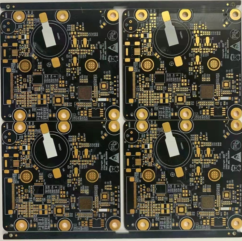
What are the benefits of using precious metals such as gold and silver on PCBs
The color is clear, let’s talk about the precious metals on the PCB! When some manufacturers promote their products, they will specifically mention that their products use special processes such as gold plating and silver plating. So what is the use of this process?
The PCB surface requires soldering components, so a part of the copper layer is required to be exposed for soldering. These exposed copper layers are called pads. The pads are generally rectangular or round with a small area.
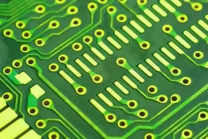
In the above, we know that the copper used in the PCB is easily oxidized, so after applying the solder mask, the copper on the pad is exposed to the air.
If the copper on the pad is oxidized, it will not only be difficult to solder, but also the resistivity will greatly increase, which will seriously affect the performance of the final product. Therefore, engineers have come up with various methods to protect the pads. For example, it is plated with inert metal gold, or the surface is covered with a layer of silver through a chemical process, or a special chemical film is used to cover the copper layer to prevent contact between the pad and the air.
For the exposed pads on the PCB, the copper layer is directly exposed. This part needs to be protected to prevent it from being oxidized.
From this perspective, whether it is gold or silver, the purpose of the process itself is to prevent oxidation, protect the pad, and ensure the yield in the subsequent soldering process.
However, the use of different metals will impose requirements on the storage time and storage conditions of the PCB used in the production plant. Therefore, PCB factories generally use vacuum plastic packaging machines to package PCBs before PCB production is completed and delivered to customers to ensure that the PCBs are not oxidized to the limit.
Before the components are soldered on the machine, the board card manufacturer must also check the oxidation degree of the PCB, remove the oxidized PCB, and ensure the yield. Finally, the boards that consumers get have undergone various tests. Even if they are used for a long time, the oxidation will almost only occur at the plug-in connection parts, and it will have no effect on the pads and soldered components.
Since the resistance of silver and gold is lower, after using special metals such as silver and gold, will the heat generation of PCB be reduced?
The factor that affects the amount of heat is resistance. The resistance is related to the material of the conductor itself, the cross-sectional area and length of the conductor. The thickness of the metal material on the surface of the pad is even far less than 0.01 mm. If the pad is processed by the OST (organic protective film) method, there will be no excess thickness at all. The resistance exhibited by such a small thickness is almost equal to 0, even impossible to calculate, and of course it will not affect the heat generation.
If you have any PCB demands, please feel free to contact us.
Email:[email protected]
Skype:[email protected]
Telephone number:+86 133 9241 2348
Whatsapp: +86 133 9241 2348