In PCB design, the pad is a very important concept, and PCB engineers must be familiar with it. However, although familiar, many engineers have little knowledge of pads.
Today, the circuit bacteria takes you to understand the types of pads and the design standards of pads in PCB design.
Pad, the basic unit of surface mount assembly, is used to form the land pattern of the circuit board, that is, various combinations of pads designed for special component types.
Partially conductive pattern of pads for electrical connection, device attachment, or both

Types of PCB Pads
- Common pads
(1) Square pads – when the components on the printed board are large and few, and the printed wires are simple, they are often used. Using this pad is easy to implement when making a PCB by hand.
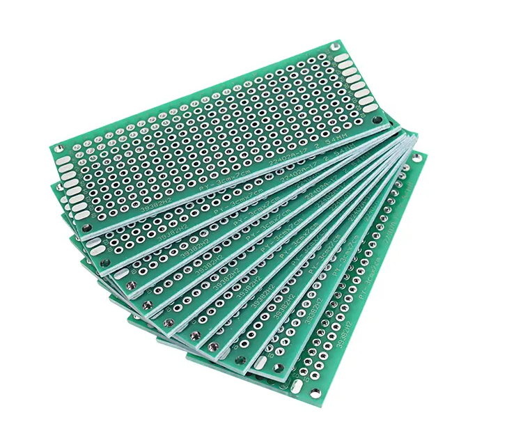
(2) Circular pads – widely used in single and double-sided printed boards with regular arrangement of components. If the density of the board allows, the pad can be larger, and it will not fall off when soldering.
(3) Island-shaped pads – the connection between the pads and the pads is integrated. Commonly used in vertical irregular arrangement installation.
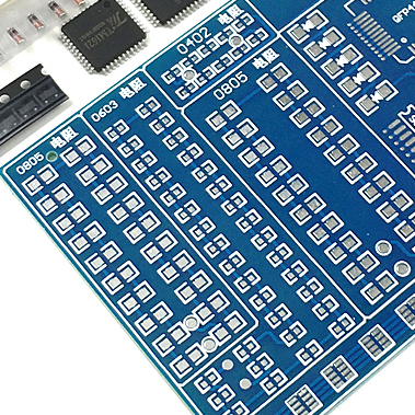
(4) Polygonal pads – used to distinguish pads with similar outer diameters and different apertures, which are convenient for processing and assembly.
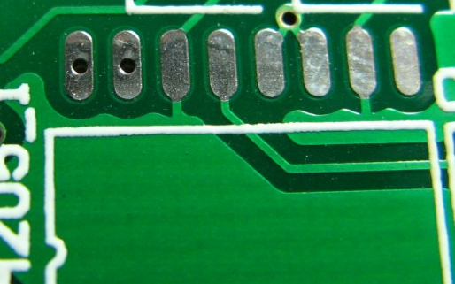
(5) Oval pads – This pad has enough area to enhance the anti-stripping ability and is often used in dual in-line devices.
(6) Open-shaped pads – in order to ensure that after wave soldering, the pad holes for manual repair welding are not blocked by solder.
- Special pad
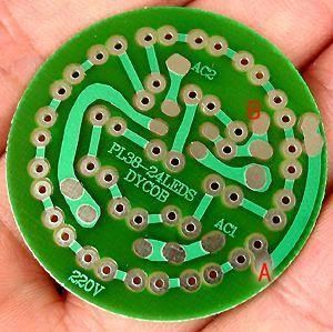
(1) Plum blossom pad
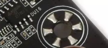
Torx pads are usually used where large vias are grounded. There are several reasons for this design:
A. The fixing hole needs to be metallized and connected to GND. If the fixing hole is fully metallized, it is easy to block the hole during reflow soldering.
B. The use of internal metal screw holes may cause the grounding to be in a poor state due to installation or multiple disassembly and assembly. The use of plum hole pads can ensure a good grounding no matter how the stress changes.
(2) Cross flower pads

Cross-shaped pads are also called thermal pads, hot air pads, etc. Its function is to reduce the heat dissipation of the pads during soldering, so as to prevent virtual soldering or PCB peeling caused by excessive heat dissipation.
A. When your pad is ground. The cross flower can reduce the area of connecting the ground wire, slow down the heat dissipation speed, and facilitate welding.
B. When your PCB needs to be patched by machine, and it is a reflow soldering machine, the cross-shaped pad can prevent the PCB from peeling (because more heat is needed to melt the solder paste).
(3) Teardrop pad
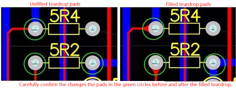
It is often used when the traces connected to the pads are thin to prevent peeling of the pads and disconnection of the traces from the pads. This type of pad is commonly used in high frequency circuits.
Design standards for pads in PCB design
- Design standards for the shape and size of PCB pads
(1) Call the PCB standard package library.
(2) The minimum single side of the pad is not less than 0.25mm, and the maximum diameter of the entire pad is not more than 3 times the diameter of the component.
(3) Try to ensure that the distance between the edges of the two pads is greater than 0.4mm.
(4) Pads with a diameter of more than 1.2mm or a pad diameter of more than 3.0mm should be designed as diamond-shaped or plum-shaped pads.
(5) In the case of relatively dense, it is recommended to use oval and oval connecting plates. The diameter or minimum width of the single-sided pad is 1.6mm; the double-sided weak current circuit pad only needs to add 0.5mm to the hole diameter, and the pad is too large to cause unnecessary continuous welding. - PCB pad via size standard
The inner hole of the pad is generally not less than 0.6mm, because the hole smaller than 0.6mm is not easy to process when punching. Usually, the diameter of the metal pin plus 0.2mm is used as the diameter of the inner hole of the pad, such as the diameter of the metal pin of a resistor. When it is 0.5mm, the diameter of the inner hole of the pad corresponds to 0.7mm, and the diameter of the pad depends on the diameter of the inner hole.
- Key points of reliability design of PCB pads
(1) Symmetry, in order to ensure the balance of the surface tension of the molten solder, the pads at both ends must be symmetrical.
(2) Pad spacing, too large or too small pad spacing will cause soldering defects, so make sure that the distance between the component ends or pins and the pads is appropriate.
(3) The remaining size of the pad, the remaining size of the component end or pin after overlapping the pad must ensure that the solder joint can form a meniscus.
(4) The width of the pad should be basically the same as the width of the component end or pin.
Any PCB and PCBA demands, please feel free to contact [email protected]!