1.Power layout and wiring related
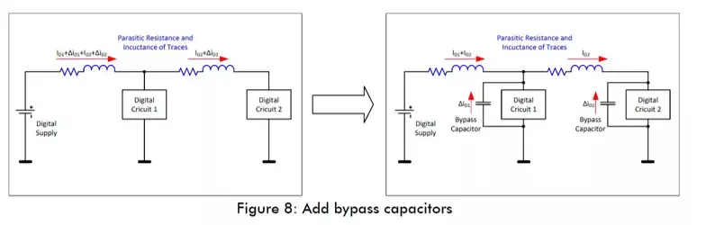
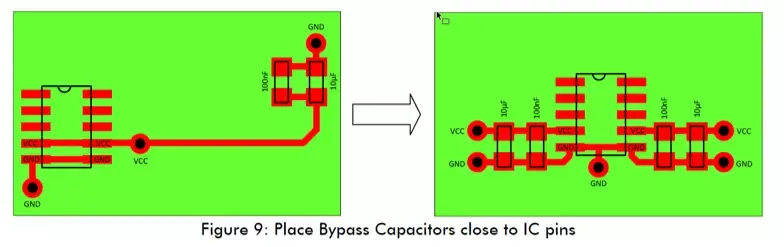
The current required by digital circuits is often discontinuous, so inrush current will be generated for some high-speed devices. If the power traces are very long, high frequency noise due to inrush current can be introduced, and this high frequency noise can be introduced into other signals. In high-speed circuits, parasitic inductance, parasitic resistance and parasitic capacitance are bound to exist, so the high-frequency noise will eventually be coupled to other circuits, and the existence of parasitic inductance will also lead to the maximum inrush current that the trace can withstand. drop, which in turn results in a partial voltage drop that may disable the circuit. Therefore, it is particularly important to add bypass capacitors in front of digital devices. The larger the capacitor is, the more energy it transmits is limited by the transmission rate, so a large capacitor and a small capacitor are generally combined to satisfy the full frequency range.
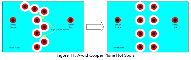
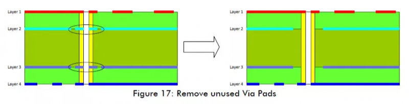
Avoid Hot Spots: Signal vias will create voids on power planes and bottom layers. Therefore, the unreasonable placement of vias is likely to increase the current density in some areas of the power or ground plane. And these places where the current density increases are called hot spots.
Therefore, we must try our best to avoid this situation when setting vias, so as to avoid the plane being split, which will eventually lead to EMC problems. Usually the best way to avoid hot spots is to place vias in a mesh pattern, so that the current density is uniform, and the planes are not isolated, the return path is not too long, and there is no EMC problem.
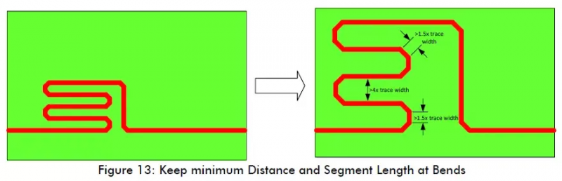
2.The way the trace is bent
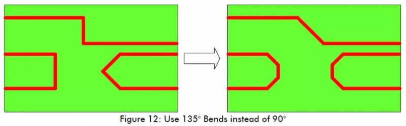
When laying high-speed signal lines, the signal lines should try to avoid bending. If you have to bend the trace, don’t run it at an acute or right angle, but use an obtuse trace.
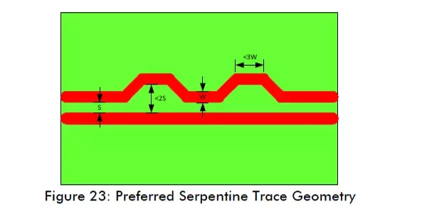
When laying out high-speed signal lines, we often use serpentine lines to achieve equal lengths, and the same serpentine lines are actually a kind of bending. The line width, spacing, and bending method should be selected reasonably, and the spacing should meet the 4W/1.5W rule.
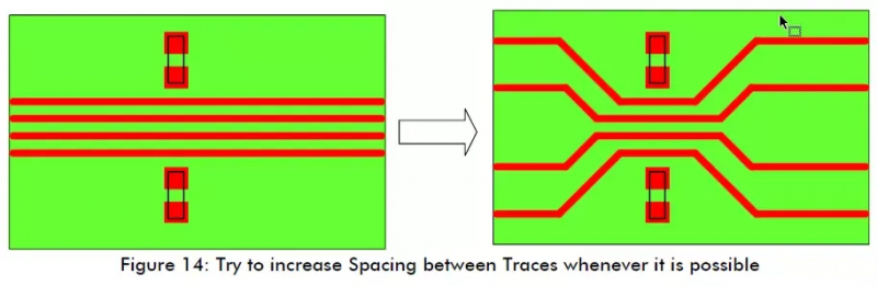
3.Proximity of the signal
If the distance between high-speed signal lines is too close, it is easy to generate crosstalk. Sometimes, due to layout, board frame size and other reasons, the distance between the high-speed signal lines exceeds our minimum required distance, so we can only try to increase the distance between the high-speed signal lines near the bottleneck. distance. In fact, if the space is enough, try to increase the distance between the two high-speed signal lines.
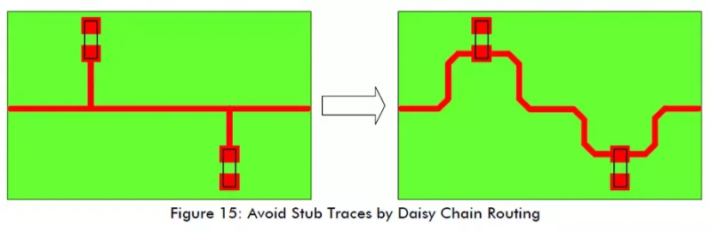
4.Trace stubs
A long stub wire is equivalent to an antenna, and improper handling can cause serious EMC problems. At the same time, the stub line will also cause reflections, reducing the integrity of the signal. Usually, when a pull-up or pull-down resistor is added to the high-speed signal line, stub lines are most likely to be generated. Generally, the stub lines can be routed in a daisy chain. According to experience, if the length of the stub line is greater than 1/10 wavelength, it can be used as an antenna, and this will become a problem.
5.Impedance discontinuity
The impedance value of a trace generally depends on its width and the distance between the trace and the reference plane. The wider the trace, the lower its impedance. In some interface terminals, which are also the pads of the device, the same principle applies. When the pad of an interface terminal is connected to a high-speed signal line, if the pad is very large at this time, and the high-speed signal line is very narrow, the impedance of the large pad is small, and the narrow trace must have a large impedance. In this case, there will be impedance discontinuities, and impedance discontinuities will produce signal reflections. Therefore, in order to solve this problem in general, a forbidden copper sheet is placed under the interface terminal or the large pad of the device, and at the same time, the reference plane of the pad is placed on another layer, thereby increasing the impedance and making the impedance continuous.
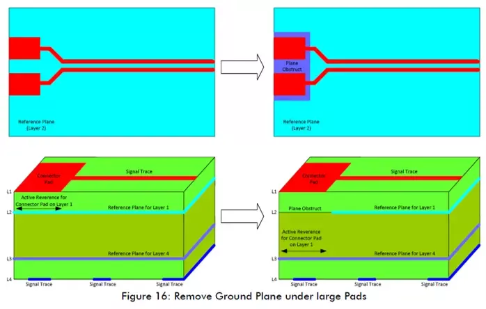
Vias are another source of impedance discontinuities. To minimize this effect, the unwanted copper layers connected to the inner layers and vias should be removed. In fact, such an operation can be used to eliminate unnecessary copper sheets through CAD tools during design or contact and communicate PCB processing maternity leave to ensure the continuity of impedance.
6.Differential signal
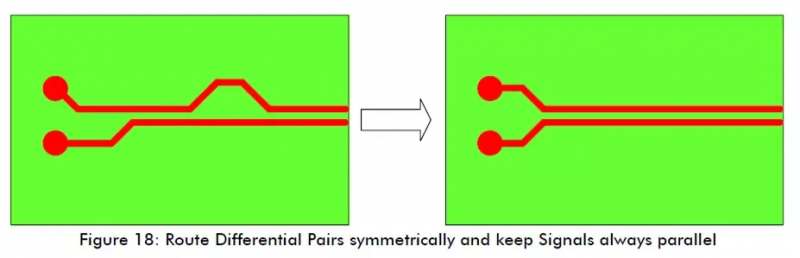
For high-speed differential signal lines, we must ensure equal width and equal spacing to achieve a specific differential impedance value. Therefore, try to ensure symmetry when laying out differential signal lines.
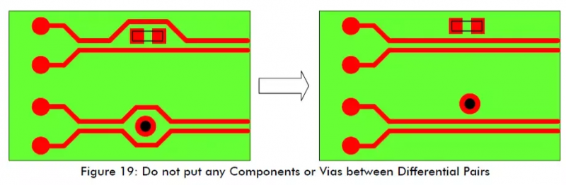
It is forbidden to place vias or components in the differential pair. If the vias or components are placed in the differential pair, it will cause EMC problems and impedance discontinuities.
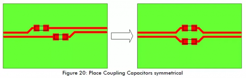
Sometimes, some high-speed differential signal lines require series coupling capacitors. The coupling capacitor also needs to be symmetrically arranged, and the package of the coupling capacitor should not be too large. It is recommended to use 0402 and 0603. It is best not to use capacitors above 0805 or side-by-side.
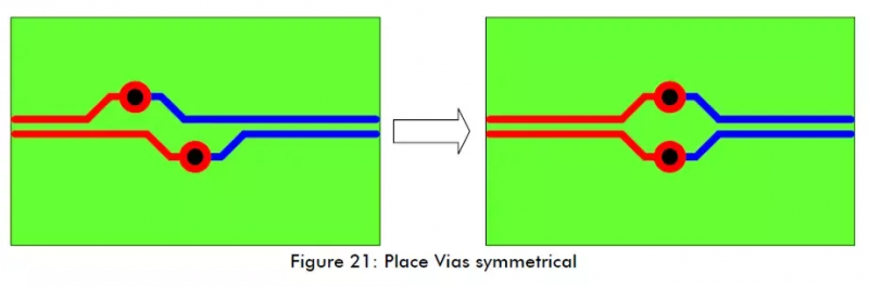
Typically, vias create huge impedance discontinuities, so for high-speed differential signal pairs, minimize vias, and use vias symmetrically if they are to be used.
7.Isometric
In some high-speed signal interfaces, such as a bus, it is generally necessary to consider the arrival time and skew error between the signal lines. For example, the arrival time of all data signal lines in a group of high-speed parallel buses must be guaranteed to be within a certain time delay error, so as to ensure the consistency of its setup time and hold time. To meet this need, we must consider isometrics.
The high-speed differential signal line must ensure a strict time delay between the two signal lines, otherwise the communication is likely to fail. Therefore, in order to meet this requirement, the serpentine line can be used to achieve the same length, thereby meeting the time delay requirement.
Serpentines should generally be placed at the source of the loss of length, not at the far end. Only at the source can the signals at the positive and negative ends of the differential line be transmitted synchronously most of the time.
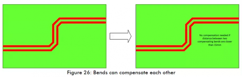
The bend of the trace is one of the sources of loss of length. For the bend of the trace, its equal length should be close to the bend (<=15mm)
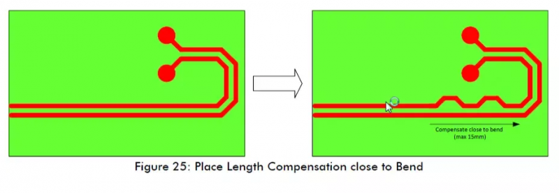
If two traces are bent and the distance between them is less than 15mm, the loss of length between the two will compensate each other, so there is no need to do equal-length processing at this time.
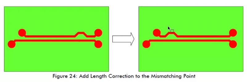
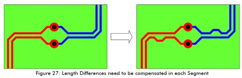
For different parts of the high-speed differential signal lines, they should be independent and equal in length. Vias, series coupling capacitors and interface terminals will be divided into two parts for high-speed differential signal lines, so special attention should be paid at this time. Must be of equal length. Because many EDA software only pays attention to whether the entire trace is long during DRC.
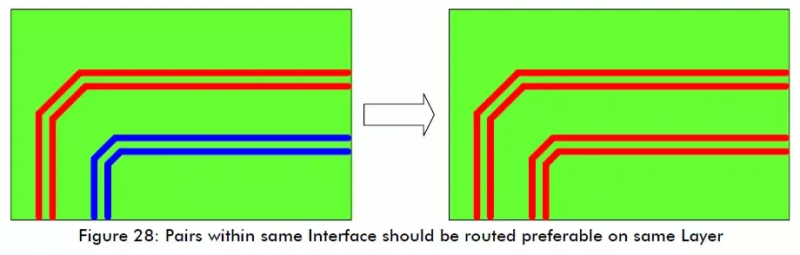
For interfaces such as LVDS display devices, there will be several pairs of differential pairs at the same time, and the timing requirements between the differential pairs are generally very strict, and the time delay requirements are particularly small. Therefore, for such differential signal pairs, we generally require them to be in the same plane. to compensate. Because the signal transmission speed of different layers is different.
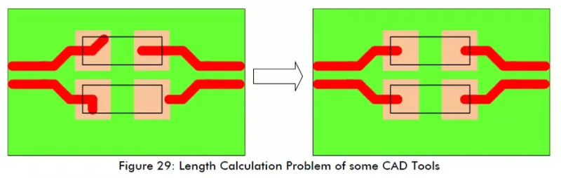
When some EDA software calculates the length of the trace, the trace inside the pad will also be calculated in the length. If the length compensation is performed at this time, the final actual result will be lost. So pay special attention at this time, when using some EDA software.
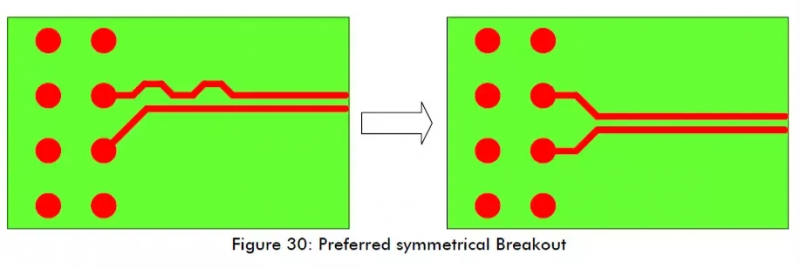
Whenever possible, choose symmetrical routing to avoid the need to end up serpentine routing for equal lengths.
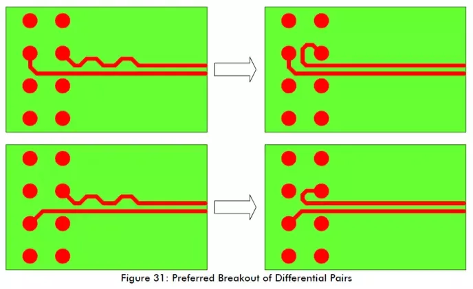
If space permits, try to compensate by adding a small loopback at the source of the short differential line instead of serpentine.
If you have any PCB demands, please feel free to contact us.
Email:[email protected]
Skype:[email protected]
Telephone number:+86 133 9241 2348
Whatsapp: +86 133 9241 2348