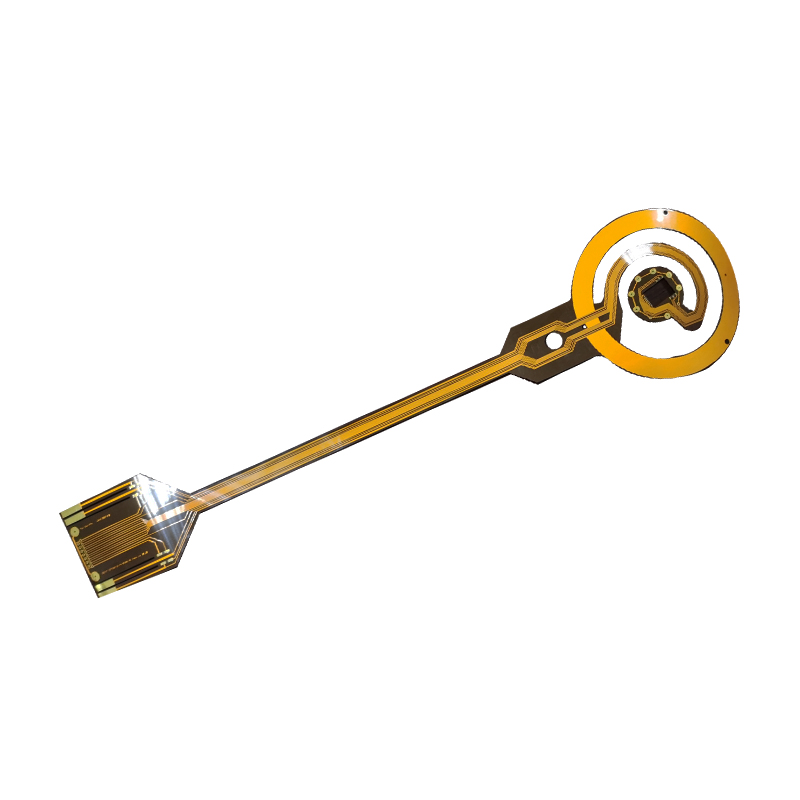
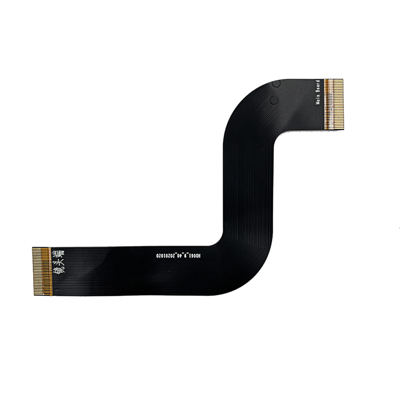
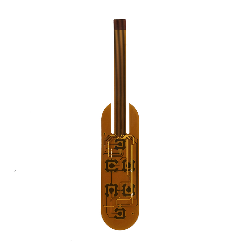
1.FPC Board cut
Except for some materials, the materials used in flexible printed boards are basically rolls. Since not all processes must be processed by the tape-and-reel process, some processes must be cut into sheets for processing, such as the drilling of metallized holes of double-sided flexible printed boards, which can only be drilled in sheet form at present. Holes, so the first process of double-sided flexible printed boards is to open the material.
Flexible copper-clad laminates have extremely poor resistance to external forces and are easily injured. If it is damaged during cutting, it will have a serious impact on the pass rate of subsequent processes. Therefore, even if it seems to be a very simple cutting, in order to ensure the quality of the material, it must be paid enough attention. If the amount is relatively small, a manual shearing machine or a hob cutter can be used, and an automatic shearing machine can be used for large batches.
Whether it is single-sided, double-sided copper foil laminate or cover film, the accuracy of the cutting size can reach ±0.33. The reliability of opening is high, and the opened materials are automatically and neatly stacked, and no personnel are required to collect materials at the exit. The damage to the material can be controlled to a minimum, and the material has almost no wrinkles and scars by using the change of the size of the feeding roller. Moreover, the latest device can also automatically cut the etched flexible printed board by the tape-and-reel process. The optical sensor can detect the corrosion positioning pattern and perform automatic cutting and positioning. The cutting accuracy is 0.3mm, but this kind of The frame of the cutting material is used as the positioning for the subsequent process.
2.FPC Drilling Vias
The through-holes of flexible printed boards can also be drilled by numerical control like rigid printed boards, but they are not suitable for hole processing of double-sided metallized hole circuits on tape and tape. With the high density of circuit patterns and the small diameter of metallized holes, and the limit of the diameter of CNC drilling, many new drilling technologies have been put into practical application. These new drilling techniques include plasma etching, laser drilling, micro-aperture punching, chemical etching, etc. These drilling techniques are easier to meet the hole-forming requirements of the tape-and-reel process than CNC drilling.
The through-holes of flexible printed boards can also be drilled by numerical control like rigid printed boards, but they are not suitable for hole processing of double-sided metallized hole circuits on tape and tape. With the high density of circuit patterns and the small diameter of metallized holes, and the limit of the diameter of CNC drilling, many new drilling technologies have been put into practical application. These new drilling techniques include plasma etching, laser drilling, micro-aperture punching, chemical etching, etc. These drilling techniques are easier to meet the hole-forming requirements of the tape-and-reel process than CNC drilling.
01 CNC drilling
Most of the drilling holes in the double-sided flexible printed boards are still drilled with CNC drilling machines. The CNC drilling machines are basically the same as those used in rigid printed boards, but the drilling conditions are different. Since the flexible printed board is very thin, multiple overlapping holes can be drilled. If the drilling conditions are good, 10 to 15 sheets can be overlapped for drilling. The backing plate and the cover plate can be made of paper-based phenolic laminate or glass fiber cloth epoxy laminate, or aluminum plate with a thickness of 0.2 to 0.4 mm can be used. Drill bits for flexible printed boards are available in the market, and drill bits for drilling rigid printed boards and milling cutters for milling shapes can also be used for flexible printed boards.
The processing conditions for drilling, milling the cover film and the shape of the reinforcing plate are basically the same, but because the adhesive used in the flexible printed board material is soft, it is very easy to adhere to the drill bit, and the drill bit status needs to be checked frequently. And the speed of the drill should be appropriately increased. Be especially careful when drilling multi-layer flexible printed boards or multi-layer rigid-flex printed boards.
02 punching
Punching micro-apertures is not a new technology and has been used for mass production. Due to the continuous production of the tape and tape process, there are also many examples of using punching to process the through holes of the tape and tape. However, batch punching technology is limited to punching holes with a diameter of 0.6-0.8mm. Compared with CNC drilling machine drilling, the processing cycle is long and requires manual operation. Because the size of the initial process is large, the punching die is correspondingly large. , Therefore, the price of the mold is very expensive. Although mass production is beneficial to reduce costs, the depreciation burden of equipment is large, and the small batch production and flexibility cannot compete with CNC drilling, so it is still not popular.
However, in recent years, great progress has been made in both die precision and numerical control drilling of punching technology, and the practical application of punching in flexible printed boards is very feasible. The latest mold manufacturing technology can produce holes with a diameter of 75um in a non-adhesive copper clad laminate with a substrate thickness of 25um, and the punching reliability is also quite high. If the punching conditions are suitable, it can even punch a diameter of 50um. hole. The punching device has also been numerically controlled, and the mold can be miniaturized, so it can be well applied to the punching of flexible printed boards. Neither numerical control drilling nor punching can be used for blind hole processing.
03 laser drilling
Lasers can be used to drill the finest through holes. Laser drilling machines used to drill through holes in flexible printed boards include excimer laser drilling rigs, impact carbon dioxide laser drilling rigs, YAG (yttrium aluminum garnet) laser drilling rigs, and argon gas. Laser rigs, etc.
The impact carbon dioxide laser drill can only drill the insulating layer of the substrate, while the YAG laser drill can drill the insulating layer and copper foil of the substrate. The speed of drilling the insulating layer is significantly higher than that of drilling the copper foil. Fast, it is impossible to use the same laser drilling machine for all drilling production efficiency. Generally, the copper foil is first etched, the pattern of the hole is formed first, and then the insulating layer is removed to form a through hole, so that the laser can drill holes with extremely small diameters. However, at this time, the positional accuracy of the upper and lower holes may restrict the hole diameter of the drilled hole. If the blind hole is drilled, as long as the copper foil on one side is etched away, there is no problem of upper and lower position accuracy. The process is similar to the plasma etching and chemical etching described below.
The pores processed by excimer lasers are currently the smallest. Excimer laser is ultraviolet light, which directly destroys the structure of the resin in the base layer, makes the resin molecules discrete, and generates very little heat, so the degree of heat damage around the hole can be limited to a minimum, and the hole wall is smooth and vertical. If the laser beam can be further reduced, holes with a diameter of 10-20um can be processed. Of course, the larger the thickness-to-aperture ratio, the more difficult the wet copper plating is. The problem with excimer laser technology drilling is that the decomposition of the polymer will produce carbon black attached to the hole wall, so some means must be taken to clean the surface before electroplating to remove the carbon black. However, when laser processing blind holes, the uniformity of the laser also has certain problems, which will produce bamboo-like residues.
The biggest difficulty of excimer laser is that the drilling speed is slow and the processing cost is too high. Therefore, it is limited to the processing of small holes with high precision and high reliability.
The impact carbon dioxide laser generally uses carbon dioxide gas as the laser source, and radiates infrared rays. Unlike excimer lasers, which burn and decompose resin molecules due to thermal effects, it belongs to thermal decomposition, and the shape of the processed holes is worse than that of excimer lasers. The hole diameter that can be processed is basically 70-100um, but the processing speed is obviously much faster than that of excimer laser, and the cost of drilling is also much lower. Even so, the processing cost is still much higher than the plasma etching method and chemical etching method described below, especially when the number of holes per unit area is large.
It should be noted that when processing blind holes, the laser can only be emitted to the surface of the copper foil, and the organic matter on the surface does not need to be removed at all. In order to stably clean the copper surface, chemical etching or plasma etching should be used as a post-treatment. Considering the possibility of technology, it is basically not difficult for the laser drilling process to be used in the tape and tape process, but considering the balance of the process and the proportion of equipment investment, it is not dominant, but the automatic welding of tape chips The width of the process (TAB, Tape Automated Bonding) is narrow, and the tape-and-reel process can improve the drilling speed, and there have been practical examples in this regard.
3.hole metallization
The hole metallization of flexible printed boards is basically the same as that of rigid printed boards.
In recent years, there has been a direct electroplating process that replaces electroless plating and adopts the technology of forming a carbon conductive layer. The hole metallization of flexible printed boards has also introduced this technology.
Because of its softness, the flexible printed board needs a special fixing fixture. The fixture can not only fix the flexible printed board, but also must be stable in the plating solution, otherwise the thickness of copper plating will be uneven, which will also cause wire breakage in the etching process. and important reasons for bridging. To obtain a uniform copper layer, the flexible printed board must be taut in the fixture, and work must be done on the position and shape of the electrodes.
For outsourcing of hole metallization, it is necessary to avoid outsourcing to factories that have no experience in FPC hole formation. If there is no special electroplating line for FPCB, the hole quality cannot be guaranteed.
4.Cleaning of copper foil surface
In order to improve the adhesion of the resist mask, the surface of the copper foil should be cleaned before applying the resist mask. Even this simple process requires special attention for flexible printed boards.
Generally, there are chemical cleaning process and mechanical grinding process. For the manufacture of precision graphics, in most cases, the two cleaning processes are combined for surface treatment. Mechanical grinding uses the method of brushing. If the brushing material is too hard, it will cause damage to the copper foil, and if it is too soft, the grinding will be insufficient. Generally, nylon brushes are used, and the length and hardness of the throwing brush must be carefully studied. Use two brush throwing rollers, which are placed on the top of the conveyor belt. The rotation direction is opposite to the belt conveying direction. However, if the pressure of the brush throwing roller is too large at this time, the substrate will be stretched by a lot of tension, which will cause dimensional changes. one of the important reasons.
If the surface treatment of the copper foil is not clean, the adhesion with the resist mask will be poor, which will reduce the pass rate of the etching process. Due to the recent improvement in the quality of copper foil boards, the surface cleaning process can also be omitted in the case of single-sided circuits. But for precise patterns below 100μm, surface cleaning is an essential process.
Coating of resist – double-sided FPC manufacturing process Now, the coating method of resist is divided into the following three methods according to the precision and yield of circuit pattern: screen printing method, dry film/photosensitive method, liquid resist Etch photosensitive method.
At present, the coating method of resist is divided into the following three methods according to the precision and output of circuit pattern: screen printing method, dry film/photosensitive method, and liquid resist photosensitive method.
The anti-corrosion ink uses the screen printing method to directly print the circuit pattern on the surface of the copper foil. This is the most commonly used technology, which is suitable for mass production and has low cost. The accuracy of the formed circuit pattern can reach the line width/spacing 0.2-0.3 mm, but it is not suitable for more precise patterns. With the miniaturization this method is gradually unable to adapt. Compared with the dry film method described below, it requires operators with certain skills, and operators must be trained for many years, which is a disadvantage.
As long as the dry film method has complete equipment and conditions, a line width pattern of 70-80 μm can be obtained. At present, most of the precision patterns below 0.3mm can be formed by dry film method to form resist circuit patterns. Using dry film, its thickness is 15 ~ 25μm, conditions permitting, the batch level can produce patterns with a line width of 30 ~ 40μm.
When choosing a dry film, it must be determined according to the compatibility with the copper foil board and process and through experiments. Even if the experimental level has good resolution, it does not necessarily have a high pass rate when used in mass production. The flexible printed board is thin and easy to bend. If a harder dry film is used, it is brittle and has poor follow-up, so cracks or peeling will occur, which will reduce the pass rate of etching.
The dry film is in roll form, and the production equipment and operation are relatively simple. The dry film is composed of a three-layer structure of a thinner polyester protective film, a photoresist film and a thicker polyester release film. Before sticking the film, first peel off the release film (also known as the diaphragm), and then press it on the surface of the copper foil with a hot roller, and then tear off the upper protective film (also known as the carrier film or cover film) before developing. Generally, there are guide positioning holes on both sides of the flexible printed board, and the dry film can be slightly narrower than the flexible copper foil board to be filmed. The automatic lamination device for rigid printed boards is not suitable for lamination of flexible printed boards, and some design changes must be made. Due to the large linear speed of dry film lamination compared with other processes, many factories do not use automatic lamination, but use manual lamination.
After sticking the dry film, in order to make it stable, it should be placed for 15-20min before exposure.
If the line width of the circuit pattern is less than 30μm, and the pattern is formed with a dry film, the pass rate will be significantly reduced. In mass production, dry film is generally not used, but liquid photoresist is used. The thickness of the coating will vary depending on the coating conditions. If a liquid photoresist with a thickness of 5 to 15 μm is coated on a copper foil with a thickness of 5 μm, the laboratory level can etch the line width below 10 μm.
Liquid photoresist must be dried and baked after coating. Since this heat treatment will have a great influence on the performance of the resist film, the drying conditions must be strictly controlled.
If you have any PCB demands, please feel free to contact us.
Email:[email protected]
Skype:[email protected]
Telephone number:+86 133 9241 2348
Whatsapp: +86 133 9241 2348