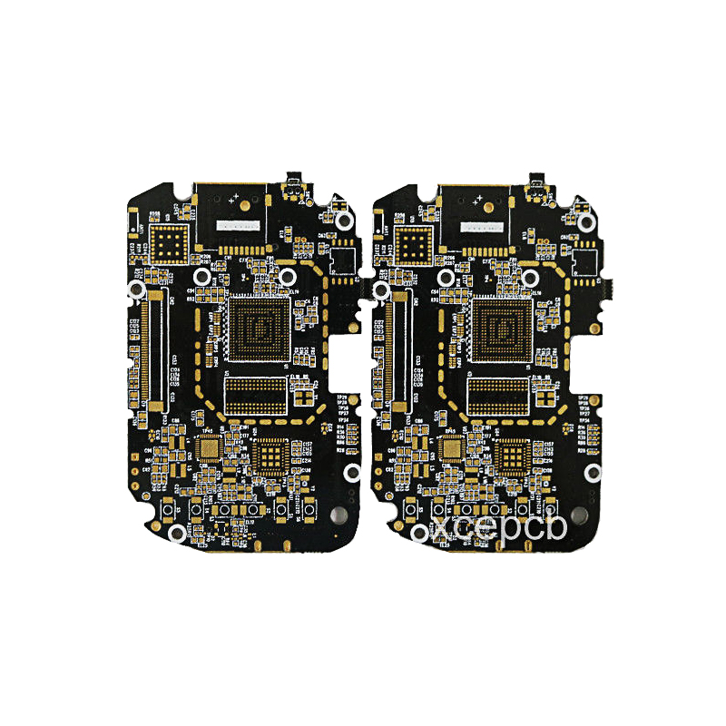
PCB proofing refers to the trial production of printed circuit boards before mass production. It is mainly used for electronic engineers to design the circuit and complete the drawing of the PCB, and then conduct a small batch trial production process to the circuit board factory, that is, PCB proofing. The following is an introduction to the preparations that need to be done before PCB proofing.
There are simple and complex PCB boards. It is not necessary to say that proofing of simple PCB boards is easy, but if it is a complex circuit board proofing, you must be cautious. It is too late to find out when the PCB board is ready. Therefore, you must make adequate preparations before proofing.

Preparations for PCB Proofing
1. Physical border production
The closed physical frame is a basic platform for future component layout and PCB proofing. Be sure to pay attention to accuracy, and it is best to use arcs at the corners, which can not only avoid being scratched by sharp corners, but also reduce the stress.
2. Introduce components and networks, and lay out components
When drawing components and networks into the drawn frame during PCB proofing, be sure to follow the prompts carefully, including the packaging form of components and network problems of components. Because of the comparison tips, it is not easy to have problems. The layout of components and traces during PCB proofing has a great impact on the product’s life, stability, and electromagnetic compatibility, and should be paid special attention to. Generally speaking, there should be the following principles: placement order, pay attention to heat dissipation.
3. PCB design, wiring and adjustment
It is best to pay attention to the requirements of processing parameters during PCB design and wiring, or to a reliable PCB proofing manufacturer, the defective rate will be greatly reduced. After completing the PCB design and wiring, all you need to do is to make some adjustments to the text, individual components, and traces and apply copper (this work should not be done too early, otherwise it will affect the speed and bring trouble to the PCB design and wiring), also for the purpose of It is convenient for production, debugging and maintenance.
4. Check the network
Sometimes the network relationship of the drawn PCB board is different from the schematic diagram due to misoperation or negligence. At this time, it is necessary to check. Therefore, after drawing, you should check it first, and then carry out follow-up work.
If you have any PCB demands, please feel free to contact us.
Email:[email protected]
Skype:[email protected]
Telephone number:+86 133 9241 2348
Whatsapp: +86 133 9241 2348