PCB multi-layer boards refer to multi-layer circuit boards used in electrical products. Multi-layer boards are wiring boards that use more single or double panels. Use one double-sided as the inner layer, two single-sided as the outer layer or two double-sided as the inner layer and two single-sided as the outer layer of the printed circuit board. The positioning system and the insulating adhesive material alternately together and the conductive pattern Printed circuit boards that are interconnected according to design requirements become four-layer and six-layer printed circuit boards, also known as multi-layer printed circuit boards.
With the continuous development of SMT (Surface Mount Technology) and the continuous introduction of a new generation of SMD (Surface Mount Devices), such as QFP, QFN, CSP, BGA (especially MBGA), electronic products are becoming more intelligent and miniaturized. Promoted major reforms and advances in PCB industrial technology.
Since IBM first successfully developed high-density multi-layer (SLC) in 1991, major groups in various countries have also developed various high-density interconnect (HDI) micro-porous plates. The rapid development of these processing technologies has prompted the design of PCBs to gradually develop in the direction of multi-layer, high-density wiring. Multi-layer printed boards have been widely used in the manufacturing of electronic products due to their flexible design, stable and reliable electrical performance and superior economic performance.
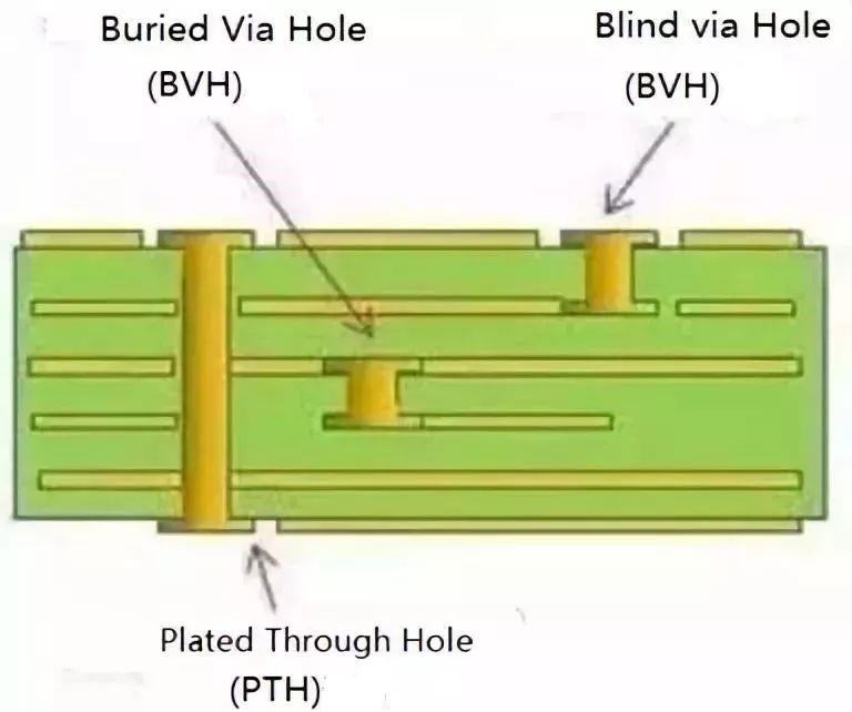
Altium Designer can provide up to 32 Signal Layers, including Top Layer, Bottom Layer and Mid-Layer. The layers can be connected to each other through Via or Through Hole, Blind Via and Buried Via.
PCB hole
Top Layer: Also called component layer, it is mainly used to place components. For double-layer boards and multi-layer boards, it can be used to lay out wires or pour copper.
Bottom Layer: Also called soldering layer, it is mainly used for wiring and soldering. For double-layer boards and multi-layer boards, it can be used to place components.
Mid-Layers: There can be up to 30 layers, which are used to arrange signal lines in a multi-layer board. Power lines and ground lines are not included here.
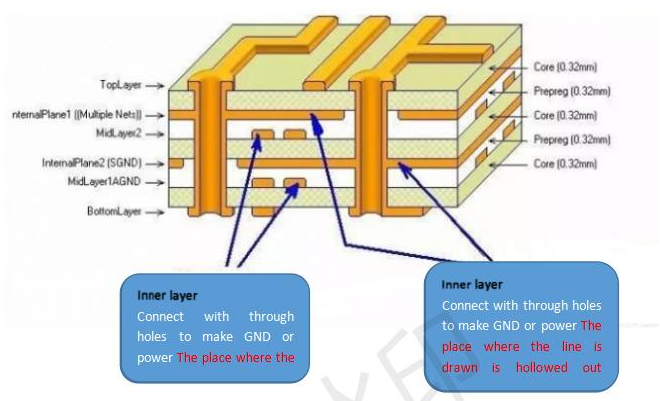
The internal power plane is usually referred to as the Internal Planes for short, which only appears in multi-layer boards. The number of PCB board layers generally refers to the sum of the signal layer and the internal plane. As with the signal layer, the inner electric layer and the inner electric layer, and the inner electric layer and the signal layer can be connected to each other through through holes, blind holes, and buried holes.
Labeling of each layer of the electrical layer in the PCB
Silk screen layer
A PCB board can have up to 2 Silkscreen Layers, which are Top Overlay and Bottom Overlay. They are generally white and are mainly used to place printed information, such as components. The outline and annotations, various annotation characters, etc., facilitate the soldering of PCB components and circuit inspection.
Top Overlay: Used to mark the projection outline of the components, the label, nominal value or model of the component, and various annotation characters.
Bottom Overlay: Same as the top silk screen. If all the labels on the top silk screen have been included, the bottom silk screen can be turned off.
Mechanical Layers
Mechanical Layers are generally used to place indicative information about board manufacturing and assembly methods, such as PCB dimensions, size markings, data materials, via information, assembly instructions and other information. This information varies according to the requirements of the design company or PCB manufacturer. The following examples illustrate our common methods.
Mechanical 1: Generally used to draw the frame of the PCB as its mechanical shape, so it is also called the shape layer.
Mechanical 2: We used to place the PCB processing process requirement form, including information such as dimensions, plates, and layers.
Mechanical 13 & Mechanical 15: The body size information of most components in the ETM library, including the three-dimensional model of the component; for the sake of simplicity of the page, this layer is not displayed by default.
Mechanical 16: The footprint information of most components in the ETM library can be used to estimate the PCB size in the early stages of the project; For the simplicity of the page, this layer is not displayed by default, and the color is black.
Altium Designer provides two types of Solder Mask and Paste Mask , which also have a top layer and a bottom layer.
Solder Mask: Solder mask refers to the part of the board that needs to be painted with green oil. Because it is a negative output, the actual effect of the part with the Solder mask is not painted with S/M, but tinned and silver-white!
Paste Mask: The solder mask layer is used for machine patching. It corresponds to the pads of all patch components. The size is the same as the Top Layer/Bottom Layer layer. It is used to open the stencil to leak tin.